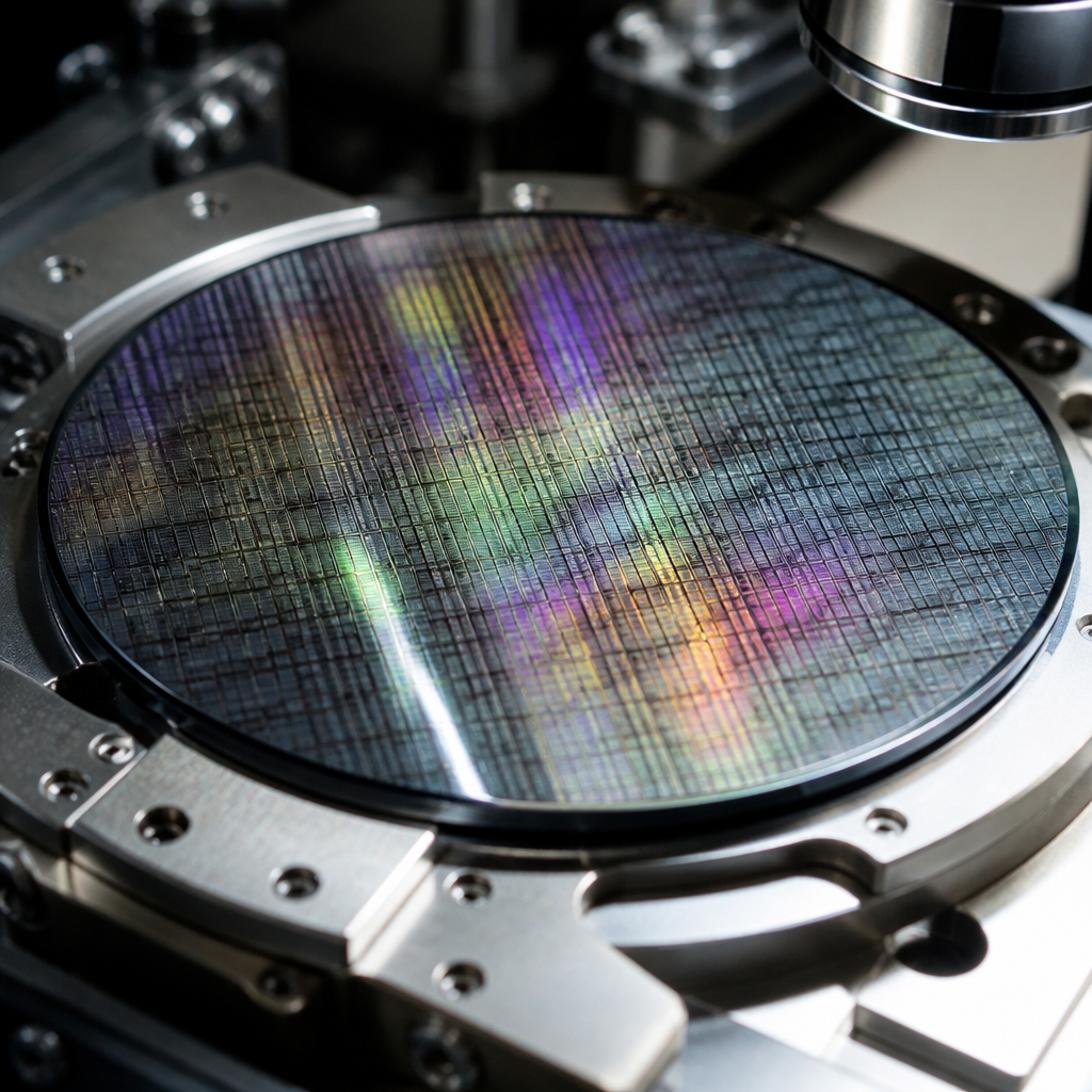
Silicon photonics is moving from a specialist engineering field into a core computing conversation because AI workloads are exposing the physical limits of conventional electrical interconnects. In simple terms, silicon photonics uses light to move data through chips and systems, often by guiding laser signals through waveguides fabricated with semiconductor manufacturing techniques. For AI computing, that matters because modern models depend not only on powerful processors but also on fast, energy-efficient data movement between memory, accelerators, servers, and racks. After working on infrastructure planning for accelerator clusters, I have seen a recurring pattern: the bottleneck is frequently not raw arithmetic throughput, but the cost, latency, and power required to feed data into that throughput.
This sub-pillar hub for semiconductors and compute explains why silicon photonics has become strategically important, how it fits into the broader chip stack, and where its opportunities and limitations sit today. The topic belongs under tech innovations and startups because it touches every layer of the market: foundries such as TSMC and Intel, networking leaders like Broadcom and Cisco, cloud operators building AI factories, and startups developing optical I/O, co-packaged optics, and photonic interposers. It also intersects with semiconductor economics, packaging, memory bandwidth, thermal design, and data center architecture. Understanding silicon photonics helps make sense of the next decade of AI hardware, where progress will come as much from moving bits better as from multiplying matrices faster.
What silicon photonics is and why AI makes it urgent
Silicon photonics combines optical components and semiconductor processes to transmit information using light rather than electrical current over selected links. A typical system includes lasers, modulators that encode electrical data onto light, waveguides that steer photons, photodetectors that convert light back into electrical signals, and control electronics. The core advantage is straightforward: optical links can carry enormous bandwidth over distance with lower signal loss and lower energy per transmitted bit than copper at comparable speeds. That statement needs nuance, though. Optical links are not universally better inside every chip block, and they still require electrical-to-optical conversion overhead. Their value rises as bandwidth demand, link distance, and power constraints increase together.
AI is exactly that scenario. Training and serving large models requires clusters of GPUs, TPUs, or custom accelerators sharing parameters, activations, and gradients across many nodes. Inside one server, high-bandwidth memory and advanced packaging keep data close to compute. Beyond that boundary, networking becomes a first-order design problem. Ethernet and InfiniBand switch fabrics have scaled impressively, but electrical interconnects over copper traces and pluggable modules face practical limits in reach, density, heat, and power. As lane speeds move from 112G PAM4 toward 224G and beyond, equalization complexity and signal integrity penalties become harder to manage. In deployment reviews, this is where photonics stops being an academic alternative and becomes a credible systems necessity.
The real bottleneck in AI computing: data movement
The popular image of AI hardware focuses on compute engines: NVIDIA GPUs, Google TPUs, AMD Instinct accelerators, and custom ASICs. Those matter, but system architects know the harder question is how quickly data can move between them. Training a frontier model can involve tens of thousands of accelerators operating in parallel. If interconnect bandwidth is insufficient or latency is too high, expensive compute sits idle waiting for communication-heavy tasks such as all-reduce operations. This is why networking companies now sit near the center of the AI value chain. The useful metric is no longer only teraFLOPS or TOPS; it is delivered application performance once memory, interconnect, and software overheads are included.
Silicon photonics addresses that bottleneck by reducing the cost of moving large volumes of data across boards, between sockets, and across racks. Optical links can support wavelength-division multiplexing, where multiple colors of light share a single waveguide or fiber, multiplying throughput without proportionally increasing physical complexity. That is powerful in dense AI clusters where front-panel space, cable bulk, and switch power all matter. It also supports a broader industry shift from monolithic scaling to system-level scaling. As transistor gains slow and advanced nodes become more expensive, better packaging and better interconnect increasingly determine real-world performance improvements.
| Compute challenge | Electrical approach | Silicon photonics advantage | Key limitation |
|---|---|---|---|
| Rack-to-rack AI bandwidth | High-speed copper and pluggables | Higher reach with lower loss and less cable bulk | Optical conversion adds cost |
| Switch port density | More retimers and larger thermal budget | Supports denser optical I/O | Packaging complexity rises |
| Power per transmitted bit | Increases sharply at higher lane rates | Better efficiency over longer links | Laser integration remains difficult |
| Scaling AI clusters | Signal integrity becomes harder over distance | Maintains bandwidth across larger fabrics | Software and network topology still matter |
How silicon photonics fits into semiconductors and compute
As the hub for semiconductors and compute, this topic should be understood in relation to the full hardware stack. At the device level, advanced logic still depends on CMOS transistors fabricated on leading nodes. Memory bandwidth comes from HBM stacks connected through advanced packaging. Chiplets and 2.5D integration, using technologies such as CoWoS and EMIB, allow more modular high-performance designs. Networking chips, including switch ASICs and NICs, move traffic inside the cluster. Silicon photonics does not replace these categories. It acts as an enabling interconnect layer that can extend the benefits of advanced compute beyond the boundaries where electrical signaling becomes inefficient.
This positioning is why major semiconductor players care. Intel has invested in silicon photonics for years, especially for data center connectivity. TSMC supports photonic integration efforts because packaging and foundry services are converging. NVIDIA’s networking strategy, strengthened by Mellanox, reflects the reality that accelerator value depends on fabric performance. Startups such as Ayar Labs have pushed optical I/O concepts that aim to bring photonics closer to the processor package, reducing the distance high-speed electrical signals must travel before converting to light. In practical architecture discussions, that step is significant because every millimeter of high-speed electrical routing adds loss, power, and design complexity.
Where the technology is used today and what changes next
Today, silicon photonics is most established in data center transceivers. These modules connect switches and servers over fiber for 100G, 400G, and increasingly 800G links. The market has matured because cloud operators need bandwidth at scale and accept optical economics where reach and density justify it. Companies such as Broadcom, Marvell, Coherent, and Cisco participate through DSPs, optical engines, switching silicon, and systems integration. In these environments, photonics already proves its practical value: lower attenuation than copper over distance, better cable manageability, and a path to higher aggregate bandwidth.
The next transition is more consequential for AI computing: bringing optics closer to the compute package through co-packaged optics and optical I/O. Co-packaged optics places optical engines near the switch ASIC, reducing the electrical trace length that would otherwise consume too much power at extreme bandwidths. Optical I/O goes further by linking processors or chiplets optically. If commercialized at scale, this could reshape board design, memory disaggregation, and cluster topology. However, these are not guaranteed near-term wins. Reliability, manufacturing yield, thermal management, fiber attach, and serviceability remain serious engineering hurdles. In other words, the direction is clear, but deployment timing depends on cost and operational maturity, not just laboratory results.
Why startups and investors are paying attention
Few semiconductor themes currently combine technical urgency, strategic relevance, and open market whitespace as strongly as photonic interconnects. Startups are targeting specific pain points rather than trying to replace the entire incumbent stack. Some focus on low-power optical I/O chiplets. Others build lasers, packaging methods, design software, or test infrastructure. That specialization makes sense because success depends on fitting into existing semiconductor and data center supply chains. A startup can create real value by solving one stubborn problem, such as coupling light efficiently into packaged devices or improving wafer-level photonic test, without needing to become a full-stack systems vendor.
Investors are interested because the demand driver, AI infrastructure, is both immediate and capital intensive. Cloud providers and model developers are spending billions on accelerator clusters, and interconnect cost increasingly shapes total cost of ownership. Even small reductions in watts per gigabit can matter at hyperscale. Still, this is not an easy category. Sales cycles are long, qualification standards are demanding, and customers expect multiyear reliability under harsh thermal conditions. Foundry access, packaging partnerships, and design-tool support can determine whether a promising photonics startup becomes a supplier or remains a science project.
The limits, tradeoffs, and what to watch next
Silicon photonics is important, but it is not magic. It does not remove the need for better memory hierarchies, more efficient AI software, or smarter parallelization strategies. For short distances on-package, electrical links may remain superior because optical conversion overhead is not free. Laser sources are still a major challenge, since silicon itself is not an efficient laser material and often requires heterogeneous integration with III-V materials. Packaging is another bottleneck. Aligning fibers, managing thermal drift, and preserving yield across complex assemblies can erase theoretical advantages if execution is poor. These are the practical realities that experienced hardware teams weigh before adopting any new interconnect technology.
What should readers track? First, watch whether co-packaged optics moves from controlled deployments into mainstream switch roadmaps. Second, monitor optical I/O pilots tied to AI accelerators and chiplet-based systems. Third, follow standards bodies and ecosystem support, because broad adoption depends on interoperable supply chains rather than one-off demonstrations. Fourth, pay attention to energy per bit and total system power, not isolated bandwidth claims. In semiconductors and compute, durable winners solve system constraints, not marketing checkboxes. Silicon photonics matters because it attacks one of AI’s hardest constraints: moving data fast enough, far enough, and efficiently enough to keep modern compute architectures productive. If you follow AI infrastructure, this is the interconnect story to watch closely over the next decade.
Frequently Asked Questions
What is silicon photonics, and why is it becoming important for AI computing?
Silicon photonics is a technology that uses light rather than electrical signals to move information through and between chips, packages, and larger computing systems. Instead of relying entirely on copper traces and electrical interconnects, silicon photonic devices guide laser light through tiny optical pathways called waveguides that are manufactured using semiconductor fabrication methods similar to those used for conventional chips. That compatibility with established chipmaking processes is one reason the field has attracted so much attention.
Its importance to AI comes from a practical bottleneck: modern AI systems are not limited only by how fast a processor can perform calculations, but also by how efficiently data can be delivered to where those calculations happen. Training and inference at scale require enormous movement of model parameters, activations, gradients, and memory traffic across accelerators, switches, and servers. Traditional electrical interconnects become harder to scale under those conditions because they consume more power, generate more heat, and face signal integrity challenges as bandwidth demands rise.
Silicon photonics is increasingly seen as a way to relieve that pressure. Optical links can move large amounts of data at high speed over longer distances with lower signal loss and potentially better energy efficiency than purely electrical approaches. In AI infrastructure, that could improve communication between GPUs, TPUs, CPUs, memory subsystems, and network fabrics. In short, silicon photonics matters because AI is pushing data movement into the spotlight, and light-based communication offers a credible path beyond some of the physical limits of electrical interconnects.
Why are conventional electrical interconnects becoming a problem for large-scale AI systems?
Electrical interconnects have served computing extremely well for decades, but AI workloads are exposing where they start to struggle. As AI models grow larger and more distributed, systems need to move vast amounts of data not just inside one chip, but across packages, boards, racks, and data centers. That communication must happen quickly and reliably, because idle processors waiting for data waste expensive compute capacity. In many advanced AI systems, the challenge is no longer simply raw compute performance; it is feeding the compute efficiently enough to keep utilization high.
The first issue is power. High-speed electrical signaling over copper becomes increasingly energy-intensive as bandwidth increases. Engineers must compensate for loss, noise, and distortion with more sophisticated signaling schemes, retimers, equalization, and other power-hungry electronics. The second issue is heat. More power devoted to moving bits means more thermal load, which is already a major constraint in dense AI servers packed with accelerators. The third issue is physical scaling. As data rates climb, maintaining signal quality across longer electrical paths becomes more difficult, which can limit system architecture flexibility.
These limitations matter directly to AI clusters, where performance depends on communication-heavy tasks such as model parallelism, distributed training, memory disaggregation, and accelerator-to-accelerator synchronization. When interconnects become bottlenecks, adding more compute does not produce proportional gains. Silicon photonics is attractive because optical communication can reduce some of these penalties, especially over distances where electrical links become increasingly inefficient. That does not make electronics obsolete, but it does mean that light-based data movement is becoming a serious option in the places where AI systems are most stressed.
How does silicon photonics actually use light to move data in AI hardware?
At a high level, silicon photonics works by encoding digital information onto beams of light and guiding that light through microscopic optical structures integrated onto or alongside semiconductor devices. A laser provides the optical source. Modulators imprint data onto the light by changing properties such as intensity or phase. The light then travels through waveguides, which are tiny pathways that confine and direct optical signals across a chip or between components. At the receiving end, photodetectors convert the optical signals back into electrical form so standard electronic logic can process them.
For AI hardware, this optical communication can be used in several places. It may connect chips within a package, accelerators across a board, servers within a rack, or systems across larger network fabrics. One major advantage is that multiple wavelengths of light can be transmitted through the same optical channel using wavelength-division multiplexing, allowing very high aggregate bandwidth without requiring a proportional increase in physical wiring. That is especially valuable in AI environments where cabling density, power consumption, and airflow all matter.
It is also important to understand what silicon photonics usually does not mean today. In most near-term AI deployments, photonics is not replacing the core arithmetic logic inside GPUs or CPUs. Instead, it is primarily enhancing data movement, which is often the real bottleneck at scale. Some researchers are exploring optical computing and photonic matrix multiplication for future AI acceleration, but the most immediate and commercially relevant role of silicon photonics is in communication: moving data faster, farther, and potentially more efficiently than traditional electrical interconnects can manage on their own.
What advantages could silicon photonics bring to AI data centers and accelerator architectures?
The most immediate advantage is higher-bandwidth communication with better scaling characteristics. AI systems increasingly depend on clusters of accelerators working together, which creates intense demand for fast, low-latency links. Silicon photonics can help support those bandwidth requirements while reducing some of the signal degradation challenges associated with high-speed electrical links. That can make it easier to build larger, more capable AI fabrics without interconnect complexity becoming the dominant design problem.
Another major benefit is energy efficiency. Data movement is becoming one of the largest contributors to power consumption in advanced AI infrastructure. Optical interconnects can lower energy per bit in certain communication scenarios, particularly over longer reaches where electrical solutions require more compensation circuitry. Even modest efficiency gains matter at hyperscale, where thousands or tens of thousands of accelerators operate simultaneously. Lower interconnect power can also ease cooling demands, improve rack density, and support more sustainable AI infrastructure economics.
Silicon photonics may also enable architectural flexibility. As interconnect constraints loosen, designers can think more creatively about disaggregated systems, shared memory pools, composable infrastructure, and tighter coupling between compute and networking. That could reshape how AI clusters are built, allowing resources to be organized for workload efficiency rather than around the strict limits of copper communication. In the longer term, silicon photonics could help support more scalable packaging strategies and more balanced system designs, where compute, memory, and networking evolve together instead of one domain outpacing the others.
What challenges are still preventing silicon photonics from becoming universal in AI computing?
Despite its promise, silicon photonics is not a simple drop-in replacement for every interconnect problem. One challenge is integration. Optical components such as lasers, modulators, couplers, and photodetectors must work reliably alongside dense electronic circuitry, advanced packaging, and demanding thermal environments. In practice, integrating these pieces at high volume and at acceptable cost remains difficult. Lasers in particular can be a sticking point, because efficient light sources are not always straightforward to incorporate directly into standard silicon processes.
There are also manufacturing, packaging, and reliability issues. Photonic systems require precise alignment and careful control over loss, temperature sensitivity, and signal quality. Small imperfections can affect performance in ways that are different from conventional electronics. In large AI deployments, operators want components that are not only fast, but also easy to manufacture, test, deploy, and maintain at scale. That means silicon photonics must prove itself not just in lab demonstrations, but in real-world supply chains and data center operating conditions.
Finally, economics and system design choices matter. Electrical interconnects are deeply entrenched, well understood, and continuously improving. In some use cases, especially over short distances, advanced electrical solutions may still be more practical or less expensive. As a result, adoption will likely happen where photonics delivers a clear advantage first, such as high-bandwidth, high-density, or longer-reach AI communication links. Over time, as AI workloads continue to expand and the pressure on power and bandwidth intensifies, silicon photonics may move from a specialized solution to a foundational technology. But that transition depends on engineering maturity, cost competitiveness, and successful integration into the broader AI hardware ecosystem.