High-bandwidth memory, usually shortened to HBM, is a specialized type of DRAM designed to move far more data than conventional memory while using less power per bit transferred. In practical terms, HBM solves a bottleneck that appears whenever processors become fast enough to wait on memory. I have seen this repeatedly in AI system design: teams focus on GPU counts, model size, and interconnects, then discover that memory bandwidth determines whether expensive accelerators stay busy or stall. That is why HBM matters. It sits at the center of modern semiconductors and compute, especially for AI training, inference, high-performance computing, and advanced graphics.
To understand HBM, it helps to define three terms. Bandwidth is the amount of data memory can deliver each second. Capacity is how much data memory can hold. Latency is how quickly memory responds to a request. Standard server DRAM, graphics memory such as GDDR6, and on-package cache all balance these factors differently. HBM is optimized primarily for extreme bandwidth and energy efficiency, achieved by stacking memory dies vertically and connecting them with through-silicon vias, or TSVs, then placing the stack close to the processor on a silicon interposer or advanced package. This architecture shortens signal paths, widens the memory interface dramatically, and reduces power compared with pushing signals across a motherboard.
For AI, this matters because transformer models, retrieval systems, recommendation engines, and simulation workloads constantly move massive tensors between compute units and memory. If the memory subsystem cannot feed matrix engines fast enough, theoretical peak FLOPS are irrelevant. The recent surge in demand for NVIDIA H100 and H200 GPUs, AMD Instinct accelerators, and custom AI chips from cloud providers is tied directly to HBM availability. In other words, HBM is not a niche component; it is a strategic constraint shaping chip roadmaps, cloud pricing, startup infrastructure choices, and national semiconductor competition.
How HBM works and why it is different
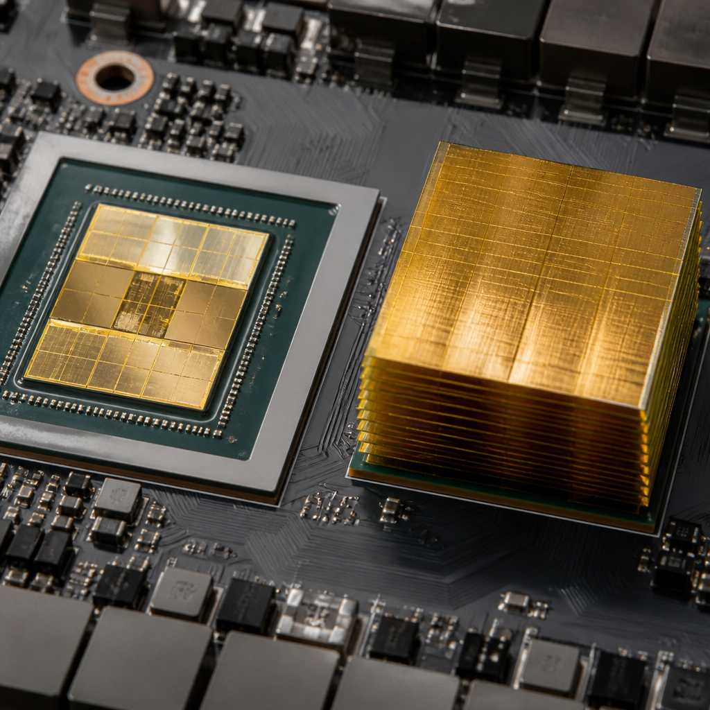
HBM achieves high throughput by going wide instead of going fast. Traditional memory often raises clock speeds to move more data, but that increases power and signal integrity challenges. HBM uses very wide interfaces, commonly 1024 bits per stack, and multiple memory channels operating in parallel. The memory dies are stacked vertically, connected through TSVs, and bonded to a base die that interfaces with the processor package. Because the memory sits next to the compute die on an interposer using 2.5D packaging, the electrical distance is much shorter than DIMMs on a motherboard. Shorter paths mean lower energy per transferred bit and more stable high-bandwidth signaling.
This design creates a different performance profile from DDR5 or GDDR6. DDR5 is excellent for general-purpose servers because it offers large capacities and flexible upgrade paths through sockets. GDDR6 is common in graphics cards because it provides high bandwidth at lower packaging complexity than HBM. HBM, however, dominates where bandwidth density matters most. AI accelerators need to read weights, activations, gradients, and optimizer states at relentless speed. A modern HBM-equipped accelerator can deliver multiple terabytes per second of memory bandwidth, a figure conventional server memory cannot approach directly. That bandwidth is often the difference between strong utilization and expensive underperformance.
The tradeoff is cost and manufacturing complexity. HBM requires advanced packaging, known-good-die testing, thermal management, and tight coordination among foundries, outsourced semiconductor assembly and test providers, and memory manufacturers such as SK hynix, Samsung, and Micron. Yield issues in any part of the stack can affect final supply. That is one reason HBM has become a strategic chokepoint across the semiconductor industry.
Why HBM is essential for AI training and inference
AI workloads are memory hungry in ways that differ from classic enterprise applications. During training, accelerators must store model parameters, intermediate activations, gradients, and optimizer states, then stream them quickly into tensor cores or matrix engines. During inference, especially with large language models, the system must serve many user requests while repeatedly accessing model weights and key-value caches. In both cases, memory bandwidth often matters as much as raw compute throughput.
Consider a large transformer. Even if the model fits in accelerator memory, each token generation step requires moving substantial data through the memory hierarchy. If memory bandwidth is insufficient, arithmetic units sit idle waiting for data. This is why AI chip vendors increasingly publish bandwidth alongside TOPS and FLOPS. NVIDIA’s H100 pairs massive compute with HBM3 because the architecture would be bottlenecked by slower memory. AMD’s Instinct MI300 family similarly emphasizes HBM capacity and bandwidth to support large models and HPC workloads. Google, Amazon, and other hyperscalers also design custom accelerators with memory systems tailored to tensor-heavy workloads.
HBM also improves efficiency. In production environments, performance per watt matters for total cost of ownership because power delivery and cooling often limit datacenter growth. Moving data consumes significant energy, sometimes more than arithmetic itself. HBM reduces the energy required per bit transferred by using shorter physical connections and lower signaling overhead. For startups renting GPU instances, this efficiency appears indirectly in cloud pricing and instance availability. For large operators, it influences rack density, thermal design, and procurement strategy.
| Memory type | Typical use | Main strength | Main limitation |
|---|---|---|---|
| DDR5 | Servers and CPUs | Capacity and upgrade flexibility | Far lower bandwidth per package |
| GDDR6 | Graphics and some accelerators | High bandwidth with simpler packaging | Less efficient and dense than HBM |
| HBM3/HBM3E | AI and HPC accelerators | Extreme bandwidth and strong energy efficiency | High cost and limited supply |
Where HBM fits in the semiconductor stack
HBM is best understood as part of a broader compute system, not a standalone upgrade. In advanced accelerators, performance depends on the interaction among the compute die, on-package memory, cache hierarchy, interconnect fabric, software stack, and workload characteristics. A chip with excellent tensor throughput can still disappoint if kernels are memory bound, if collective communication is inefficient, or if the model is sharded poorly across devices. In practice, HBM is one layer in a tightly integrated system architecture.
Packaging is the key enabler. TSMC’s CoWoS platform has become especially important because it supports the advanced packaging methods used in many leading AI accelerators. As demand for accelerator modules rose, CoWoS capacity became a visible industry constraint, affecting delivery timelines for cloud providers and startups alike. This is one reason investors and operators now pay attention not just to foundry nodes like 5 nanometer or 3 nanometer, but also to packaging capacity, interposer availability, and HBM supply agreements.
For a semiconductors and compute hub, HBM connects naturally to several adjacent topics. It intersects with GPU architecture because tensor core utilization depends on memory feed rates. It links to chiplets because future designs increasingly disaggregate compute functions while keeping memory close. It ties into datacenter networking because model parallelism can shift pressure from local memory bandwidth to cluster interconnects such as NVLink, NVSwitch, InfiniBand, and Ethernet with RoCE. It also matters for startups building inference infrastructure, since serving efficiency depends on the balance among HBM capacity, bandwidth, and software techniques like quantization and paging.
HBM generations, economics, and industry constraints
HBM has evolved through several generations, from early HBM and HBM2 to HBM2E, HBM3, and HBM3E. Each generation increases per-stack bandwidth, improves signaling, and usually raises capacity. The recent move to HBM3E is especially significant for AI because larger memory footprints and faster transfer rates support bigger models and better accelerator utilization. Yet technical progress does not guarantee abundant supply. HBM remains one of the hardest components in the AI hardware bill of materials.
The economics are shaped by concentration and complexity. A small number of suppliers dominate the market, and qualification cycles are demanding. Memory stacks must meet strict thermal and reliability requirements when attached to high-power GPUs or custom accelerators. Packaging partners need enough capacity, and the final modules must be validated across firmware, drivers, and system boards. Any bottleneck can constrain shipments. That is why earnings calls from NVIDIA, AMD, SK hynix, Samsung, Micron, TSMC, and major cloud providers increasingly discuss memory and packaging rather than only logic process nodes.
For buyers, the implication is clear: benchmark headline compute, but model system bottlenecks and supply risk. A startup choosing accelerators for model training should compare not just listed FLOPS, but effective memory bandwidth, available HBM capacity, software maturity, and lead times. I have seen teams overbuy theoretical compute and underinvest in profiling. The better approach is to map workload behavior first, then select hardware based on tokens per second, time to train, utilization, and total cost of ownership.
What comes next for HBM and AI infrastructure
HBM will remain central as AI models grow and as inference becomes more stateful, multimodal, and latency sensitive. Future accelerators will likely pair more HBM with smarter memory hierarchies, larger caches, and better compression or sparsity handling. At the same time, the industry will keep exploring alternatives and complements, including processing-in-memory concepts, silicon photonics for faster interconnects, near-memory compute, and packaging advances that place logic and memory even closer together.
The essential point is simple: compute breakthroughs depend on data movement, and HBM is the most important mainstream answer to that challenge today. If you follow semiconductors and compute, understand HBM first. It explains why certain GPUs dominate AI, why packaging capacity can move stock prices, why cloud instances are scarce, and why memory vendors suddenly shape the future of machine learning. Use this hub as your starting point, then dig deeper into accelerators, packaging, networking, and model optimization to make better technology and investment decisions.
Frequently Asked Questions
What is HBM, and how is it different from traditional DRAM?
HBM, or high-bandwidth memory, is a specialized form of DRAM built to deliver extremely fast data movement between memory and processors such as GPUs, AI accelerators, and other high-performance chips. The key difference is not just the memory cells themselves, but how the memory is physically packaged and connected. Traditional DRAM, including familiar technologies like DDR memory, typically sits farther away from the processor on a memory module or motherboard and relies on narrower interfaces running at high speeds. HBM takes a different approach: it stacks multiple memory dies vertically and places them very close to the processor, often on the same package, using a very wide memory interface. That combination allows HBM to move much more data at once while using less power per bit transferred.
In practical terms, traditional memory designs often force system architects to choose between bandwidth, power efficiency, physical space, and complexity. HBM improves that tradeoff by shortening the distance data must travel and massively increasing the width of the connection. For AI and high-performance computing, that matters because modern accelerators can process enormous amounts of data in parallel. If memory cannot feed those compute units quickly enough, the processor spends valuable time waiting. HBM is designed specifically to reduce that waiting, which is why it has become such an important feature in advanced AI hardware.
Why does high-bandwidth memory matter so much for AI workloads?
AI workloads are often limited not only by raw compute power, but by how quickly models, activations, weights, gradients, and intermediate tensors can be moved in and out of memory. A modern GPU or accelerator may contain an enormous number of parallel compute units capable of performing operations at extraordinary speed, but those units are only useful if they stay fed with data. When memory bandwidth is too low, the processor stalls, utilization drops, and overall performance falls far short of what the hardware should be able to deliver on paper. HBM addresses exactly that problem by supplying data at a much higher rate than conventional memory architectures can typically provide.
This becomes especially important in both AI training and inference. During training, large models repeatedly read and update huge parameter sets while also handling activations, optimizer states, and gradient calculations. During inference, especially for large language models and multimodal systems, the accelerator still needs rapid access to model weights and cached data to maintain low latency and high throughput. In both cases, insufficient memory bandwidth can turn expensive compute hardware into an underused asset. That is why experienced AI system designers pay close attention not only to FLOPS, GPU count, and interconnect speed, but also to how much memory bandwidth is available per accelerator. HBM is often the reason high-end AI chips can deliver the real-world performance that large-scale workloads demand.
How does HBM improve performance while using less power per bit transferred?
HBM improves performance primarily by using a very wide data path rather than depending solely on higher clock speeds. Instead of pushing data through relatively narrow channels at extreme frequencies, HBM moves data across many lanes in parallel. This wide-interface design allows it to achieve very high total bandwidth efficiently. Because the memory is placed physically close to the processor, often through advanced packaging technologies and silicon interposers, the electrical paths are shorter and signaling can be more power-efficient. Shorter distances reduce the energy required to move data, which is a major advantage in systems where power and thermals are tightly constrained.
That efficiency matters a great deal in AI infrastructure. Moving data can consume a substantial portion of system power, and in many modern workloads, data movement is just as important as arithmetic performance. If a chip can perform trillions of operations per second but wastes too much energy fetching data, the overall system becomes harder to cool, more expensive to operate, and less scalable in dense data center deployments. HBM helps reduce that burden by delivering high throughput with better energy characteristics than many traditional memory approaches. The result is not just faster hardware, but hardware that can sustain performance more effectively under real operational conditions.
Is HBM only important for very large AI models and top-tier GPUs?
HBM is most visible in top-tier GPUs and advanced AI accelerators, but its importance is not limited to only the largest systems. Any workload that needs to move large volumes of data quickly can benefit from higher memory bandwidth. That includes large model training, large language model inference, recommendation systems, graph analytics, scientific computing, and many forms of real-time data processing. Even when a model is not enormous by current frontier standards, memory bandwidth can still be a decisive factor in determining latency, throughput, and accelerator utilization.
That said, HBM is typically used where the performance gains justify the higher packaging complexity and cost. Not every AI deployment requires it. Some edge systems, smaller inference workloads, or cost-sensitive deployments can perform well with more conventional memory architectures. But once workloads become highly parallel and data-intensive, memory bandwidth often emerges as a bottleneck long before theoretical compute limits are reached. In that sense, HBM is not just a premium feature for the biggest chips; it is a strategic solution for a class of problems where feeding the processor efficiently is essential to extracting real value from the hardware.
What role does HBM play in overall AI system design and scalability?
HBM plays a foundational role because it directly affects how efficiently each accelerator can perform useful work. In AI system design, it is easy to focus on headline metrics such as the number of GPUs, total parameter count, or network fabric speed. Those are important, but they do not replace local memory performance. Each accelerator still needs rapid access to data to keep its compute engines busy. If local memory bandwidth is constrained, adding more compute does not automatically solve the problem. In fact, it can make inefficiencies more expensive by increasing the amount of idle hardware in the system. HBM helps ensure that the compute resources inside each accelerator are matched by enough data delivery capacity to support them.
Its impact also extends to scalability. In multi-accelerator clusters, strong local memory bandwidth reduces pressure on other parts of the system because more work can be completed efficiently on each device before needing external communication. That can improve training efficiency, inference throughput, and overall cost effectiveness. For system architects, HBM is part of a broader balance among compute, memory capacity, memory bandwidth, interconnect bandwidth, software optimization, and workload characteristics. When that balance is wrong, systems underperform despite impressive specifications. When it is right, HBM becomes one of the enabling technologies that allows advanced AI hardware to deliver consistent, high-value performance at scale.