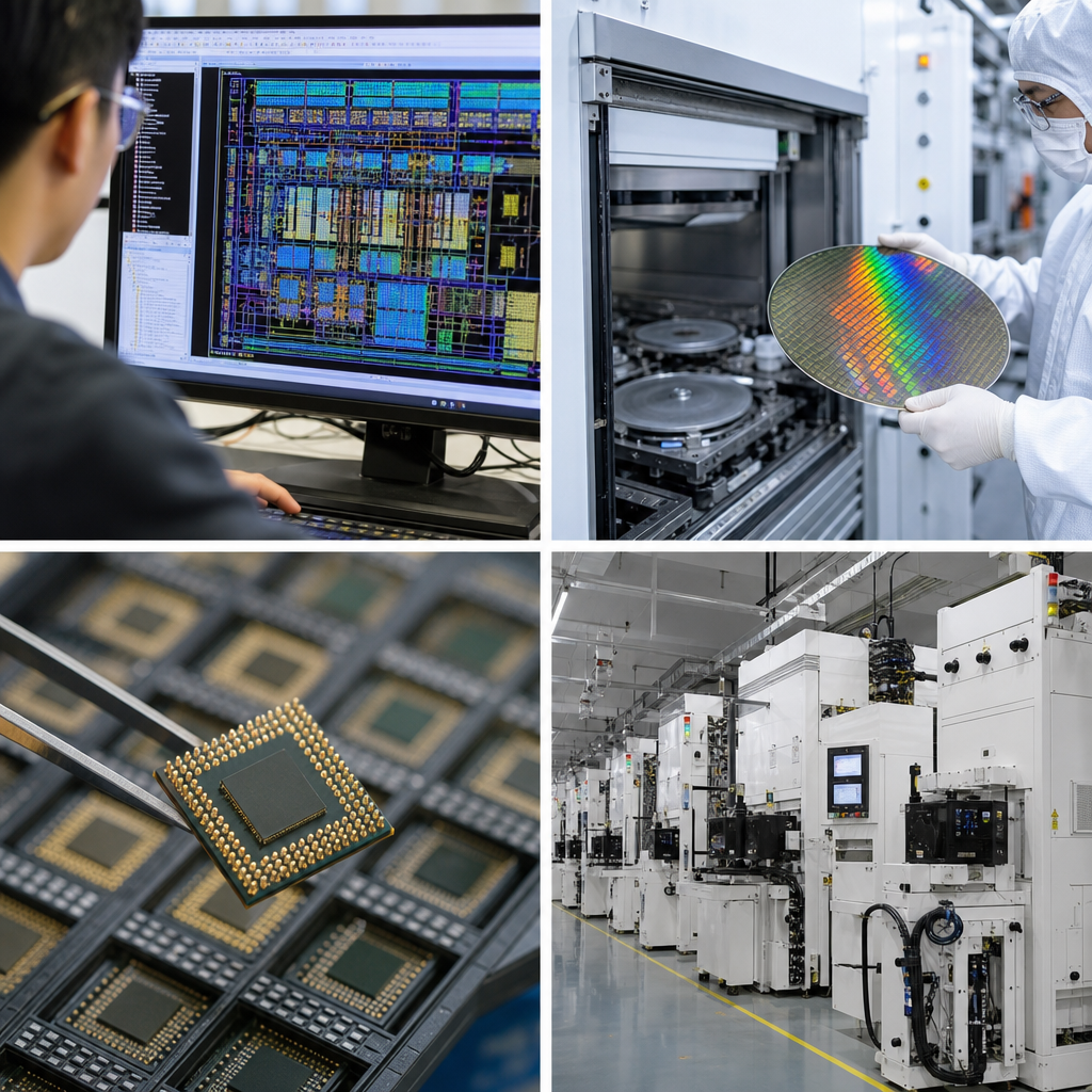
The semiconductor supply chain is the industrial system that turns a chip idea into a finished processor, memory device, power controller, or sensor, and it spans design software, intellectual property, fabrication plants, packaging houses, test operations, and the highly specialized equipment that makes every step possible. In practical terms, this chain connects fabless designers such as NVIDIA and Qualcomm, integrated device manufacturers such as Intel, foundries such as TSMC and GlobalFoundries, equipment leaders such as ASML, Applied Materials, Lam Research, KLA, and Tokyo Electron, and outsourced assembly and test companies including ASE and Amkor. When people ask why semiconductors matter, the shortest accurate answer is that nearly every modern product depends on them: smartphones, vehicles, cloud servers, industrial robots, medical devices, payment terminals, telecom networks, and defense systems all run on chips. Understanding how the semiconductor supply chain works matters because shortages, export controls, natural disasters, or delays at any single stage can ripple across entire economies.
Semiconductors are materials, usually silicon, whose electrical conductivity can be precisely controlled. A chip is a patterned arrangement of transistors, interconnects, memory cells, and other structures built onto a wafer through hundreds or thousands of process steps. The supply chain begins long before manufacturing, with electronic design automation software from companies such as Synopsys, Cadence, and Siemens EDA, plus licensable processor cores and interface blocks from Arm, Imagination, and Rambus. It continues through wafer fabrication, where foundries print and etch microscopic features, then through assembly, packaging, and final test, where bare dies become usable components. My experience following chip programs is that success depends less on one breakthrough machine than on orchestration: design rules, process recipes, yield learning, materials purity, metrology, logistics, and customer demand must all line up. That is why this sector deserves to be treated as infrastructure, not just another manufacturing category.
Chip design: where products, process limits, and economics first meet
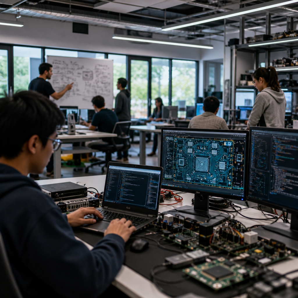
Semiconductor design translates product requirements into a manufacturable blueprint. A team starts with an architecture decision, such as CPU, GPU, accelerator, analog front end, radio, memory, microcontroller, or mixed-signal system-on-chip. Engineers then write register-transfer level code, build verification environments, perform synthesis, floorplanning, placement, routing, timing closure, power analysis, and physical verification, and finally tape out a layout file for manufacturing. This is where the first hard supply chain dependency appears: advanced chips cannot be designed competitively without EDA software, process design kits, and reusable IP blocks. For example, a startup building an AI inference chip may license Arm CPU cores, PCIe controllers, and high-speed SerDes IP, then use Synopsys or Cadence flows to target a 5 nanometer process. If any of those dependencies are delayed, the launch slips.
Node selection is one of the most misunderstood decisions. Leading-edge nodes such as 3 nanometer or 5 nanometer offer higher transistor density and often better power efficiency, but they also bring much higher mask costs, tighter design rules, and greater verification burden. Many successful products do not need the newest node. Automotive microcontrollers, power management chips, image sensors, and industrial analog devices often remain on 28 nanometer, 40 nanometer, 65 nanometer, or larger geometries because reliability, cost, embedded nonvolatile memory, and long product lifecycles matter more than density. Texas Instruments and Infineon illustrate this clearly in power and analog markets. In practice, the best design choice is the one that meets performance, cost, thermal, and volume targets with acceptable yield risk, not the one with the smallest headline number.
Foundries and wafer fabrication: how designs become silicon
Foundries manufacture wafers for chip companies that do not own fabs, while integrated device manufacturers both design and manufacture some of their own chips. TSMC dominates advanced logic foundry capacity, Samsung Foundry is a major rival, and GlobalFoundries, UMC, SMIC, Tower Semiconductor, and others serve important segments across mature logic, specialty processes, radio frequency, analog, and embedded memory. Wafer fabrication itself is a sequence of deposition, lithography, etch, ion implantation, cleaning, planarization, and inspection steps repeated layer by layer in ultra-clean environments. At advanced nodes, extreme ultraviolet lithography is central because it enables smaller features with fewer patterning steps than deep ultraviolet methods. A single fab can cost tens of billions of dollars and require years to ramp, which explains why capacity cannot be added quickly during shortages.
Yield is the governing metric in fabrication. A wafer may contain hundreds or thousands of dies, but only a percentage will meet specifications. Small process variations, contamination, mask defects, line edge roughness, overlay errors, or weak design margins can reduce that percentage sharply. During yield ramp, engineers rely on statistical process control, in-line inspection, parametric testing, and failure analysis to identify defect sources. In 2021 and 2022, the automotive shortage showed how fragile this stage can be. Carmakers canceled orders early in the pandemic, consumer electronics demand surged, and foundry capacity was reallocated. Because automotive semiconductors often need long qualification cycles and older nodes that were already capacity constrained, the supply gap persisted far longer than many executives expected. The lesson was straightforward: wafer capacity planning must reflect product criticality, not just short-term forecasts.
Packaging, assembly, and test: the overlooked stage now driving performance
After wafer fabrication, dies are singulated, attached to substrates or lead frames, interconnected, encapsulated, and tested. This stage was once viewed mainly as a commodity backend function, but advanced packaging has turned it into a performance enabler. Technologies such as flip-chip, wafer-level packaging, fan-out, 2.5D interposers, and 3D stacking allow more bandwidth, lower latency, better power delivery, and heterogeneous integration. AMD’s chiplet strategy is the clearest mainstream example. Instead of building one very large monolithic die, AMD combines multiple chiplets in one package, improving yield economics and product flexibility. High bandwidth memory stacked next to AI accelerators is another example, used in products from NVIDIA and AMD to feed massive compute engines.
Assembly and test providers including ASE, Amkor, JCET, and SPIL play a critical role here, but so do substrate suppliers and memory partners. Advanced packaging often depends on Ajinomoto build-up film substrates, through-silicon vias, microbumps, and precise thermal design. Test is equally important because chips must be screened for functionality, performance bins, and reliability. In automotive and industrial applications, qualification standards, burn-in requirements, and traceability can be demanding. The rise of chiplets means package design now affects system architecture directly. I have seen product discussions where package escape routing, thermal resistance, and substrate availability became as decisive as transistor performance. That shift is why any serious semiconductor supply chain analysis must treat packaging as a strategic capability, not a finishing step.
Equipment, materials, and chokepoints: the tools behind every transistor
No part of the semiconductor supply chain exists without production equipment and materials. Lithography systems from ASML, deposition tools from Applied Materials and Tokyo Electron, etch tools from Lam Research, process control systems from KLA, and specialty tools across cleaning, implantation, and metrology define what fabs can actually produce. The supply base also includes silicon wafers from Shin-Etsu and SUMCO, photoresists and advanced chemicals from Japanese and global suppliers, industrial gases, sputtering targets, specialty polymers, and ultrapure water systems. Because these inputs are highly specialized, substituting suppliers is difficult and slow. That is one reason export controls and sanctions have outsized effects in this industry: the bottleneck is often a unique machine, material formulation, or software capability rather than generic factory labor.
| Supply chain stage | Primary players | Main bottleneck | Real-world impact |
|---|---|---|---|
| Design | Synopsys, Cadence, Arm | EDA access and IP licensing | Delayed tape-outs and fewer competitive startups |
| Wafer fabrication | TSMC, Samsung, GlobalFoundries | Fab capacity and yield ramp | Lead-time spikes for CPUs, MCUs, and radios |
| Packaging and test | ASE, Amkor, JCET | Advanced substrate and OSAT capacity | AI accelerator shipment constraints |
| Equipment | ASML, Applied Materials, Lam, KLA | Long tool lead times and export controls | Slower fab expansion and regional imbalance |
Geography matters because semiconductor manufacturing is globally distributed but unevenly concentrated. Taiwan leads in advanced logic foundry, South Korea in memory and advanced manufacturing, Japan in materials and equipment components, the Netherlands in lithography, the United States in design, EDA, equipment, and high-performance processors, and China in a rapidly expanding but still constrained domestic ecosystem. Governments now treat this map as a strategic vulnerability. The U.S. CHIPS and Science Act, the European Chips Act, and major programs in Japan, South Korea, India, and China all aim to increase resilience. Yet resilience is not the same as self-sufficiency. Building a domestic fab without local talent pipelines, equipment support, reliable power, water, substrates, and customers does not create a durable ecosystem. The industry remains interdependent by design.
How startups and buyers should read the semiconductor supply chain
For startups in semiconductors and compute, the supply chain determines strategy as much as product vision. A new chip company must decide whether to build a full custom device, use an FPGA first, license standard IP, or target a mature node to control cost and risk. It also needs realistic plans for tape-out schedules, mask budgets, packaging choices, test development, and software enablement. Many first-time teams underestimate nonrecurring engineering costs and the calendar time required for validation and yield learning. The strongest startups usually narrow the problem: they target a specific workload, choose proven interfaces, partner early with foundries and OSATs, and secure packaging capacity before launch. Buyers should apply the same discipline in reverse by asking suppliers about node dependence, dual sourcing, substrate exposure, lifecycle support, and qualification status.
The semiconductor supply chain is best understood as a stack of tightly linked capabilities rather than a straight line from design to finished chip. Design tools set the boundaries of what can be built, foundries determine manufacturability and scale, packaging increasingly shapes system performance, and equipment suppliers enable every technical advance underneath. For readers following semiconductors and compute, this hub topic connects directly to AI accelerators, cloud infrastructure, edge devices, automotive electronics, and defense technology because all of them inherit the same constraints. The central takeaway is simple: chip leadership depends on coordination across design, manufacturing, packaging, materials, and policy, not on one company acting alone. If you cover tech innovations or evaluate startup opportunities, use this framework to analyze where value is created, where bottlenecks form, and where the next competitive edge will emerge.
Frequently Asked Questions
What is the semiconductor supply chain, and why is it so important?
The semiconductor supply chain is the full industrial network that transforms a chip concept into a working product used in computers, smartphones, cars, industrial systems, medical devices, and communications infrastructure. It begins with chip architecture, electronic design automation software, and licensed intellectual property blocks such as CPU cores, interface controllers, and memory designs. From there, it moves into manufacturing, where silicon wafers are processed in fabrication plants using hundreds of tightly controlled steps. After fabrication, chips are packaged, tested, validated, and shipped to device makers that integrate them into finished electronics.
Its importance comes from the fact that no modern digital economy can function without it. Semiconductors are foundational components for AI accelerators, cloud servers, consumer electronics, defense systems, and energy management hardware. If one part of the chain is disrupted, the effects ripple quickly across multiple industries. A shortage in wafers, packaging capacity, lithography tools, specialty gases, or test equipment can delay entire product lines. That is why the semiconductor supply chain is often described not as a single industry, but as a deeply interconnected ecosystem where design firms, foundries, equipment suppliers, material providers, and packaging specialists all depend on one another.
How do fabless companies, foundries, and integrated device manufacturers differ from one another?
These business models define who designs chips, who manufactures them, and who controls the production process. Fabless semiconductor companies focus primarily on chip design, product definition, software enablement, and customer relationships. Companies such as NVIDIA and Qualcomm are well-known examples. They typically do not own large fabrication plants, so they rely on outside manufacturing partners to build their chips. This model allows them to invest more heavily in architecture, performance, and market specialization without taking on the enormous capital cost of operating a leading-edge fab.
Foundries are the companies that specialize in manufacturing chips for others. TSMC and GlobalFoundries are prominent examples. A foundry takes a customer’s design files and produces wafers using specific process technologies, such as advanced logic nodes, mature nodes, RF processes, or specialty manufacturing platforms. Foundries are essential because modern semiconductor fabrication requires tens of billions of dollars in capital investment, highly specialized process expertise, and access to advanced tools such as extreme ultraviolet lithography systems, deposition equipment, etchers, and metrology systems.
Integrated device manufacturers, or IDMs, combine design and manufacturing under one organization. Intel is a classic example, although business models in the industry continue to evolve. An IDM may design its own processors, memory products, or analog chips and produce them in its own factories. This can offer tighter control over product optimization, manufacturing timelines, and long-term technology strategy. However, it also requires sustained investment across both product innovation and manufacturing operations. In practice, the industry now includes hybrid approaches as well, with some IDMs using external foundries for selected products and some design companies taking a more hands-on role in manufacturing planning.
What happens between chip design and a finished semiconductor device?
Once a semiconductor company has defined the functionality of a chip, the design process moves through architecture, logic implementation, verification, physical design, and signoff. Engineers use electronic design automation tools to simulate the chip, validate performance, check power use, and ensure the design can be manufactured reliably. They may also integrate licensed IP blocks for standard functions such as memory interfaces, high-speed connectivity, or processor cores. When the design is complete, the final data is prepared for tape-out, which is the handoff to the manufacturing side of the supply chain.
At the fabrication stage, a foundry or IDM processes silicon wafers through many complex steps. These include deposition of thin films, lithography to pattern features, etching to remove selected material, ion implantation to modify electrical behavior, chemical mechanical planarization to flatten surfaces, and repeated metrology and inspection to confirm precision. The wafer may go through this cycle dozens or even hundreds of times depending on the complexity of the chip. The result is a wafer containing many copies of the same integrated circuit.
After wafer fabrication, the chips move to assembly, packaging, and test. Individual dies are cut from the wafer, attached to substrates or lead frames, connected electrically through wire bonding or advanced interconnect methods, and enclosed in protective packaging. Increasingly, advanced packaging techniques such as chiplets, 2.5D integration, and 3D stacking are becoming critical to performance and power efficiency. Final test checks whether each device meets specifications for speed, power, functionality, and reliability. Only then are the chips shipped to system manufacturers for integration into finished products.
Why are semiconductor packaging and test so important in the supply chain?
Packaging and test are often misunderstood as final, lower-value steps, but in reality they are essential to chip performance, reliability, and manufacturability. Packaging protects the delicate silicon die from heat, moisture, contamination, and mechanical stress while also providing the electrical connections needed for the chip to communicate with the outside world. In older generations of the industry, packaging was often treated mainly as a protective shell. Today, it has become a strategic area of innovation because advanced packages can directly improve bandwidth, latency, power delivery, thermal performance, and overall system integration.
This matters especially for high-performance computing, AI accelerators, memory-intensive devices, and compact mobile systems. Advanced packaging technologies can place multiple dies in a single package, connect logic and memory more closely, and enable heterogeneous integration where chips built on different process technologies work together as one system. That means packaging is no longer just about enclosure. It is increasingly part of the product architecture itself.
Testing is equally important because even tiny process variations can affect whether a chip functions correctly under real-world conditions. Test operations screen for defects, verify performance, and sort devices by characteristics such as clock speed, leakage, and power consumption. Reliability testing can also simulate thermal stress, voltage fluctuation, and long-term operating conditions. Without robust packaging and test, manufacturers would face higher failure rates, weaker yields, and greater risk in end markets such as automotive, aerospace, and data center infrastructure where reliability standards are extremely demanding.
What role do semiconductor equipment and materials suppliers play in the overall ecosystem?
Equipment and materials suppliers are the backbone of the semiconductor supply chain because chip manufacturing is only possible through extraordinarily specialized tools and inputs. Semiconductor fabrication plants depend on lithography systems, deposition tools, etchers, ion implantation machines, metrology platforms, inspection systems, wafer handling automation, and testing equipment. Each category involves years of engineering development and must operate at extreme levels of precision. In advanced manufacturing, tiny deviations measured in nanometers can affect yield, performance, and cost.
Materials are just as critical. Fabs require high-purity silicon wafers, photoresists, specialty gases, chemicals, sputtering targets, slurries, masks, substrates, and packaging materials. These inputs must meet exacting standards for purity, consistency, and compatibility with tightly tuned manufacturing processes. If a material supplier encounters quality problems or shipping disruptions, production can slow or stop altogether. That is one reason semiconductor resilience has become a major topic for governments and manufacturers alike.
The equipment side of the ecosystem also shapes the pace of technological progress. Advances in lithography, process control, and packaging tools often determine how quickly the industry can move to smaller nodes, higher transistor density, and more complex integration methods. In other words, semiconductor leadership is not driven only by the companies that design chips or operate foundries. It also depends on the less visible but absolutely indispensable firms that build the machines and materials that make the entire chain possible.