Advanced packaging has moved from a back-end manufacturing detail to a front-line driver of computing progress, especially in the race to build faster, more efficient AI systems. In semiconductor terms, advanced packaging refers to the methods used to connect multiple chips, memory stacks, and specialized dies into a single high-performance assembly. Instead of relying only on shrinking transistors on one monolithic die, chipmakers now improve performance by arranging, stacking, and interconnecting silicon in smarter ways. That shift matters because modern AI workloads demand immense bandwidth, lower latency, and manageable power consumption, all at scales traditional packaging cannot support.
I have seen this change firsthand in how semiconductor roadmaps are discussed. A decade ago, most conversations centered on process nodes such as 10nm, 7nm, or 5nm. Today, serious engineering discussions just as often focus on 2.5D integration, 3D stacking, chiplets, through-silicon vias, substrate capacity, and high-bandwidth memory. These are not niche manufacturing topics. They determine whether a GPU can feed thousands of parallel compute units fast enough for large language model training, whether a data center can improve performance per watt, and whether a startup can bring a specialized accelerator to market without the cost and risk of building a giant monolithic chip.
As the hub for semiconductors and compute, this article explains what advanced packaging is, why it is essential to the AI boom, which technologies matter most, where the supply chain is constrained, and what business leaders, founders, and technical buyers should watch next. If you want to understand why AI hardware progress now depends as much on packaging innovation as transistor scaling, start here.
What advanced packaging means in practical terms
Traditional semiconductor packaging protects a chip and connects it to a circuit board. Advanced packaging goes further by turning the package itself into a high-performance system architecture layer. In practice, that means placing multiple compute dies, memory dies, I/O dies, or analog components extremely close together and linking them with dense, short interconnects. The result is far higher data transfer rates and lower energy per bit than a conventional board-level connection can deliver.
The key concept is that distance matters. Electrical signals lose efficiency and add latency as they travel longer paths. By shortening those paths inside the package, designers can move data faster while using less power. That is crucial for AI chips, which are often starved not by arithmetic capability but by memory bandwidth and data movement limits. An accelerator can have enormous theoretical throughput, yet underperform if it cannot keep tensor cores or matrix engines supplied with data.
Advanced packaging also changes product strategy. Rather than building one very large die, companies can split functions into chiplets: separate pieces of silicon optimized for compute, memory interface, I/O, or networking. Those chiplets can be manufactured on different process nodes and assembled into one package. AMD’s chiplet strategy in CPUs and data center processors demonstrated the economic value of this model, and AI accelerators now follow similar principles. The package has become a platform for system-level design.
Why AI workloads made packaging a bottleneck and a breakthrough
AI training and inference stress hardware differently from traditional enterprise software. Large language models, recommender systems, and multimodal models move vast amounts of data among compute units, caches, and memory. That makes bandwidth and latency central design constraints. High-bandwidth memory, or HBM, became the preferred answer because it places DRAM stacks close to the processor and connects them through a very wide interface. But HBM only works at scale because advanced packaging techniques integrate those memory stacks with GPUs and accelerators in tight physical proximity.
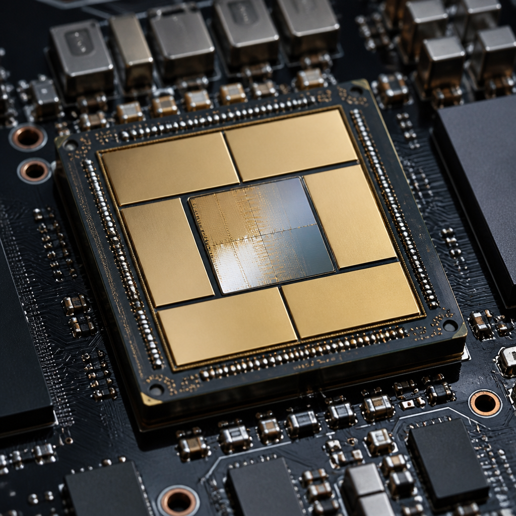
NVIDIA’s highest-end AI accelerators are a clear example. Their performance gains do not come solely from more transistors or better cores; they depend heavily on packaging schemes that combine large compute dies with HBM stacks on advanced substrates or silicon interposers. TSMC’s CoWoS technology has become widely discussed because it enables precisely this kind of integration. When industry reports mention CoWoS shortages, they are really describing a packaging capacity constraint that can limit AI server shipments even when chip demand is surging.
Power is the second reason packaging matters. Data movement often consumes more energy than computation itself. Keeping memory close to compute reduces that burden. Thermal design is the third factor. Densely packed devices generate intense heat, and successful advanced packaging must manage power delivery, heat dissipation, signal integrity, and mechanical stress at once. In AI hardware, packaging is not an afterthought. It is the enabling layer that makes leading performance possible.
The main advanced packaging technologies shaping semiconductor competition
Several packaging approaches now define the semiconductors and compute landscape. 2.5D packaging places multiple dies side by side on an interposer, often silicon, allowing dense interconnects without full vertical stacking of logic dies. This approach is common in AI accelerators that pair compute silicon with HBM. 3D packaging stacks dies vertically, using through-silicon vias to create direct electrical connections between layers. That can deliver even shorter paths and greater density, though thermal and manufacturing challenges are higher.
Chiplet-based design is the strategic architecture enabled by these packaging methods. Instead of forcing all functions onto one reticle-limited die, companies partition systems into modular dies. Intel’s Foveros, TSMC’s SoIC and CoWoS, and Samsung’s X-Cube are leading examples of named platforms supporting this direction. Each reflects a broader industry reality: packaging technology now influences competitive position as much as front-end lithography.
Another important layer is the substrate. Organic substrates, redistribution layers, bump pitch, and advanced assembly processes all affect yield, routing density, and cost. In many boardroom conversations, people talk about GPU supply as if wafer starts are the only issue. In practice, ABF substrate availability, HBM stack supply from memory vendors such as SK hynix, Samsung, and Micron, and outsourced semiconductor assembly and test capacity can all become chokepoints. The semiconductor value chain is only as strong as its packaging ecosystem.
How leading companies are using advanced packaging
The competitive landscape becomes easier to read when viewed through packaging choices.
| Company | Packaging approach | Why it matters for AI |
|---|---|---|
| NVIDIA | 2.5D integration with HBM on advanced interposers | Delivers the memory bandwidth required for large-scale model training |
| AMD | Chiplet architectures across CPUs and accelerators | Improves yield, modularity, and product scaling across markets |
| Intel | Foveros and EMIB heterogeneous integration | Combines multiple process technologies in one package |
| TSMC | CoWoS and SoIC manufacturing services | Acts as a crucial enabler for fabless AI chip companies |
NVIDIA relies on advanced packaging to turn raw silicon capability into usable AI system performance. Without close integration between GPU dies and HBM, its accelerators would be bottlenecked by memory access. AMD uses chiplets to balance economics and performance across EPYC processors and AI products, proving that modular design can be both commercially and technically powerful. Intel has invested heavily in packaging as a way to integrate different dies and reclaim system-level advantages, especially where heterogeneous computing matters.
For startups, advanced packaging opens a door but also raises the bar. A new AI chip company can use a chiplet strategy to reduce die risk and target a specific workload such as inference, edge AI, or networking offload. However, gaining access to premium packaging capacity, validating thermals, and coordinating foundry, substrate, memory, and assembly partners requires capital and operational maturity. Packaging is now a strategic moat, not just a manufacturing step.
Constraints, tradeoffs, and what comes next
Advanced packaging is powerful, but it is not magic. It introduces real tradeoffs in cost, yield, testing complexity, and thermal management. More dies and more interconnect density can mean more opportunities for assembly defects or performance variability. Known-good-die strategies, robust design-for-test methods, and co-optimization among silicon, package, and system teams are essential. In my experience, organizations that treat packaging as a late-stage handoff usually lose time and margin. The best teams design the package and the chip together from the start.
Another limitation is ecosystem concentration. A small number of foundries and OSAT providers control much of the most advanced capacity, while HBM supply is concentrated among a few memory leaders. That creates strategic risk for hyperscalers, startups, and governments seeking resilient compute supply. It also explains rising interest in domestic semiconductor incentives, supply chain diversification, and long-term capacity agreements.
Looking ahead, expect more 3D integration, better power delivery, optical interconnect experimentation, and tighter coupling between compute, memory, and networking. AI model growth will keep pushing architects toward system-level innovation. For anyone tracking semiconductors and compute, the lesson is straightforward: transistor scaling still matters, but advanced packaging is now the technology that turns silicon potential into AI reality. Follow the packaging roadmap, study the supply chain, and you will understand where the next wave of AI performance will come from.
Frequently Asked Questions
What is advanced packaging in semiconductors, and why is it so important for AI?
Advanced packaging is the set of technologies used to combine multiple semiconductor components—such as logic chips, memory, I/O dies, and accelerators—into one tightly integrated system. Rather than treating packaging as a simple protective shell around a finished chip, modern semiconductor design uses packaging as a performance tool. In practical terms, that means placing chiplets side by side, stacking dies vertically, and connecting them with ultra-short, high-bandwidth pathways so they can behave more like one coordinated device.
That matters enormously for AI because AI workloads are both compute-hungry and data-hungry. Training and inference systems need to move massive amounts of data between processors and memory with as little delay and power loss as possible. Traditional approaches that rely on one large monolithic chip run into limits involving cost, manufacturing yield, power delivery, and memory bandwidth. Advanced packaging helps overcome those bottlenecks by enabling architectures that put high-bandwidth memory closer to compute, split complex designs into specialized chiplets, and improve overall system efficiency.
In other words, advanced packaging has become one of the main ways the semiconductor industry continues to increase real-world performance even as transistor scaling becomes more difficult and expensive. For AI systems in particular, it is no longer a back-end assembly step—it is a core design strategy that directly shapes speed, energy efficiency, scalability, and product economics.
How is advanced packaging different from traditional chip packaging?
Traditional chip packaging focused primarily on protecting a finished die and providing electrical connections between the chip and the circuit board. Its role was important, but mostly supportive. The chip itself carried the bulk of the innovation, while the package served as a housing and interface layer. Performance gains mainly came from making transistors smaller and fitting more of them onto a single die.
Advanced packaging changes that model. Instead of building everything into one large silicon die, manufacturers can divide functions across multiple smaller dies and integrate them inside one package. These dies may include CPU cores, GPU elements, AI accelerators, cache, analog functions, and stacked memory. The package is no longer passive—it becomes an active part of the architecture by enabling dense interconnects, shorter signal paths, and more efficient power and thermal management.
Technologies such as 2.5D packaging, 3D stacking, fan-out packaging, silicon interposers, and hybrid bonding all fall under the advanced packaging umbrella. These methods allow much higher connection density than conventional board-level communication. The result is better bandwidth, lower latency, and often better power efficiency. For AI chips, this can mean the difference between a processor that is constrained by data movement and one that can fully utilize its compute resources.
Another key difference is manufacturing flexibility. With traditional packaging, a defect in a large monolithic die can make the whole chip unusable. With advanced packaging and chiplet-based design, companies can improve yields by manufacturing smaller dies separately and then integrating known-good components into one package. That can reduce cost, shorten development cycles, and make it easier to mix process nodes tailored to different functions.
What role do chiplets and 3D stacking play in advanced packaging for AI hardware?
Chiplets and 3D stacking are two of the most important building blocks in modern advanced packaging. A chiplet is a smaller functional die designed to work with other chiplets inside a single package. Instead of creating one giant chip that handles every task, designers can break the system into modular pieces—for example, compute chiplets, memory controllers, I/O dies, or specialized AI engines. Those chiplets are then linked through high-speed interconnects that are much faster and more efficient than traditional motherboard-level connections.
This modular approach is especially valuable in AI hardware because different workloads benefit from different forms of specialization. One chiplet can be optimized for matrix math, another for memory access, and another for communications. Manufacturers can also mix and match technologies, using cutting-edge process nodes where they matter most and more mature, lower-cost nodes where they make better economic sense. That improves flexibility while helping control manufacturing complexity and cost.
3D stacking adds another level of integration by placing dies on top of one another instead of only side by side. This can dramatically shorten the distance between compute and memory, which is critical in AI systems where memory bandwidth is often a major bottleneck. High-bandwidth memory, or HBM, is one of the best-known examples. By stacking memory dies and placing them very close to the processor, manufacturers can deliver the rapid data flow needed for large AI models.
The advantage is not just speed. Shorter connections can also reduce energy consumption per bit moved, which is crucial in large-scale AI data centers where power use is a strategic concern. The tradeoff is that stacking and dense integration create serious engineering challenges in heat dissipation, testing, assembly precision, and long-term reliability. Even so, chiplets and 3D packaging are now central to how leading AI processors are designed and scaled.
Why has advanced packaging become more critical as Moore’s Law slows down?
For decades, the semiconductor industry relied heavily on Moore’s Law and traditional scaling: make transistors smaller, fit more onto a chip, and gain improvements in performance, power efficiency, and cost per function. That model still matters, but progress is no longer as straightforward or as economical as it once was. As process nodes become more advanced, manufacturing complexity rises sharply, costs increase, and the benefits of each new node can be harder to capture across an entire large chip.
Advanced packaging has emerged as one of the most effective ways to keep performance moving forward when scaling alone is not enough. Instead of depending entirely on one monolithic die built at the most advanced node, companies can partition designs into smaller dies and integrate them in a sophisticated package. This approach helps sidestep the yield penalties and cost issues associated with very large chips, while still delivering high system-level performance.
For AI, this shift is even more important because the limiting factor is often not raw transistor count, but the ability to move data efficiently among compute units and memory. Advanced packaging directly addresses that issue by increasing interconnect density and reducing the physical distance signals must travel. In many modern AI systems, architectural innovation at the package level contributes as much to performance gains as transistor improvements on the die itself.
Put simply, advanced packaging is one of the industry’s main answers to the end of easy scaling. It allows semiconductor companies to keep improving throughput, bandwidth, and efficiency by optimizing how chips are assembled into systems. That is why packaging has moved from a secondary manufacturing concern to a strategic technology frontier.
What are the biggest challenges and future opportunities in advanced packaging?
The biggest challenges in advanced packaging revolve around heat, complexity, cost, and standardization. AI chips consume large amounts of power, and when multiple dies are packed closely together—or stacked vertically—thermal management becomes much harder. Excess heat can reduce performance, shorten component life, and limit how densely systems can be integrated. Solving that requires advances in materials, cooling approaches, package design, and power delivery.
Manufacturing complexity is another major issue. Aligning and bonding multiple dies with extremely fine interconnects demands exceptional precision. Testing also becomes more difficult because failure can occur at the die level, the interconnect level, or the package level. As packages become more heterogeneous, integrating logic, memory, analog, and photonic components, the challenge grows further. Supply chain coordination is also critical, since advanced packaging often involves specialized equipment, outsourced assembly partners, and tightly controlled production flows.
Cost remains a balancing factor. While advanced packaging can improve yields compared with a single oversized die, the packaging process itself can be expensive, especially for cutting-edge methods like 3D stacking and high-density interposer-based designs. Companies must weigh whether the performance benefits justify the added manufacturing and design overhead. In AI markets, the answer is often yes, but cost discipline still matters, particularly as deployment expands beyond elite data center hardware into broader enterprise and edge applications.
Looking ahead, the opportunities are substantial. Advanced packaging could enable even more modular chip ecosystems, where interoperable chiplets from different vendors are combined into custom systems. Improvements in hybrid bonding, optical interconnects, thermal materials, and power delivery could make future AI hardware faster and more efficient than today’s designs. As AI models continue to scale and new workloads emerge, advanced packaging will likely remain one of the most important levers for innovation across performance, energy use, and system architecture.