Lam Research sits at the center of semiconductor manufacturing, supplying the wafer fabrication equipment that allows advanced chips to move from design files to physical devices at production scale. In Silicon Valley company spotlights, Lam Research deserves close attention because it illustrates how the region’s influence extends far beyond consumer brands and software platforms. The company builds systems used for plasma etch, thin film deposition, strip, and clean processes, all of which shape and prepare the microscopic structures inside memory and logic chips. When people ask what powers semiconductor production, the answer often includes lithography leaders, design software vendors, and foundries, but the production line also depends on process equipment makers like Lam. I have worked around semiconductor content and manufacturing supply chains long enough to see one pattern repeatedly: when device architectures change, equipment capability becomes a strategic bottleneck. That is why Lam Research matters not only as a public company, but as a Silicon Valley institution whose tools influence the pace of innovation across data centers, smartphones, automotive electronics, and artificial intelligence hardware.
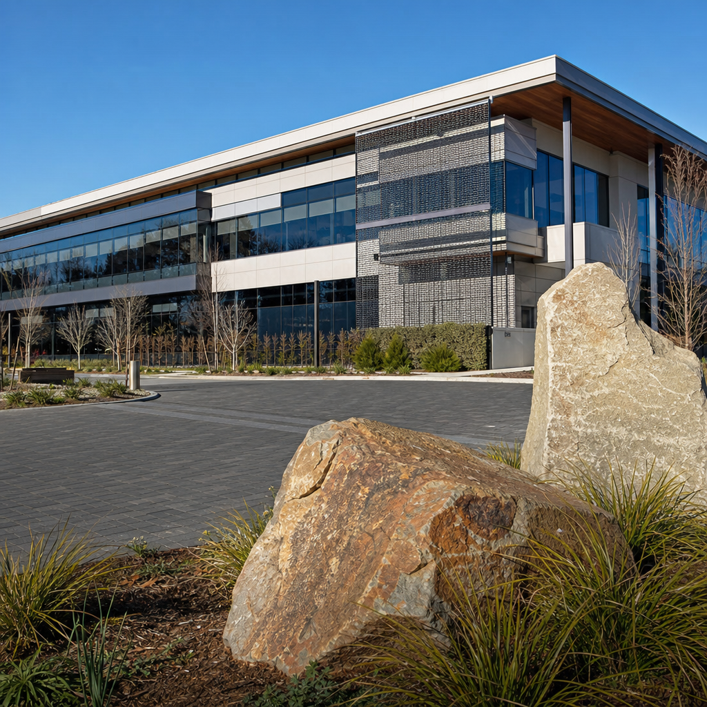
Founded in 1980 and headquartered in Fremont, California, Lam Research develops and services equipment used in front-end wafer fabrication. Front-end fabrication refers to the repeated process steps that create transistors, memory cells, interconnects, and insulating layers on silicon wafers before packaging and testing begin. Lam’s customers include leading chipmakers and foundries that require tight process control, high throughput, and predictable yield. Yield means the percentage of chips on a wafer that meet specification; even a small yield gain can be worth millions of dollars in a high-volume fab. This article serves as a hub for Company Spotlights in Silicon Valley by using Lam Research as a lens on the broader ecosystem: how semiconductor companies create value, why supply chain specialization matters, what investors and industry readers should watch, and how one company’s technology decisions can ripple through the global electronics market.
What Lam Research Actually Does in a Fab
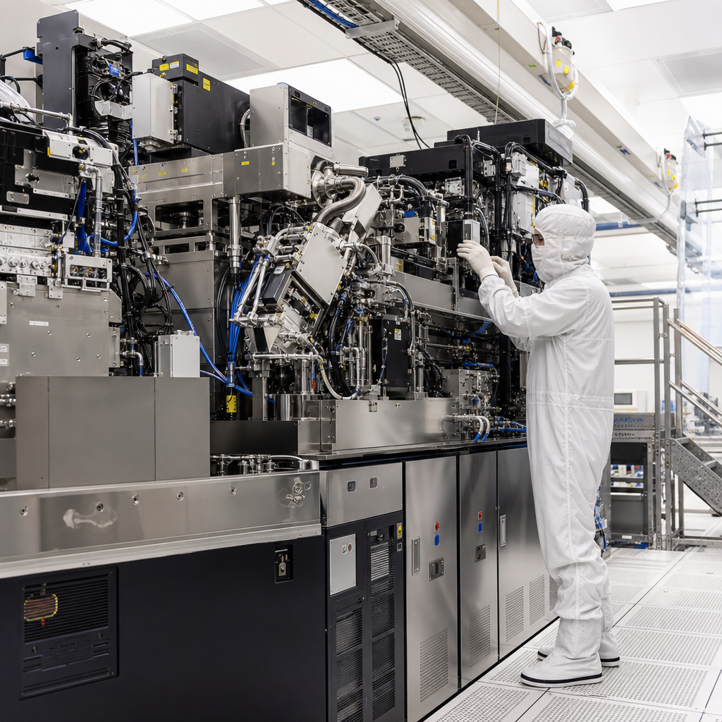
Lam Research is best known for equipment that removes and deposits material at nanometer scale with extreme precision. In etch, the company’s systems use plasma chemistry to carve patterns and high-aspect-ratio features into films on a wafer. In deposition, Lam adds thin layers of materials that act as conductors, insulators, or barriers. In clean and strip, it removes photoresist residues and contaminants that would otherwise degrade device performance. These process steps are not optional support functions; they are core manufacturing stages that determine line width control, defect density, and electrical behavior. When chip structures became three-dimensional, especially in NAND flash and advanced logic, etch and deposition complexity increased sharply. Lam benefited because it had deep capability in exactly those areas.
A simple way to understand Lam’s role is to compare a semiconductor fab to a precision machine shop operating at atomic tolerances. Designers define the target architecture, lithography exposes patterns, but process equipment turns those patterns into durable structures over hundreds or thousands of manufacturing steps. A 3D NAND device, for example, may require deep channel holes etched through stacked layers with uniformity across the wafer. If the etch profile varies, memory cells fail or performance drifts. Lam’s value comes from making those features repeatable in high-volume manufacturing, not just in laboratory demonstrations. That distinction is essential in semiconductor production, where consistency across millions of chips determines commercial success.
Why Lam Research Matters in Silicon Valley Company Spotlights
Silicon Valley company spotlights often focus on software, internet platforms, or device brands, yet the region’s industrial identity is equally rooted in semiconductor infrastructure. Lam Research represents the capital equipment layer of that infrastructure. Its presence in Fremont places it in a network of suppliers, engineers, researchers, and customers that has shaped the Valley for decades. While some manufacturing has shifted globally, the concentration of technical expertise, product management, and process innovation in Silicon Valley remains significant. Lam is a reminder that the Valley still matters because it develops the tools that define what advanced manufacturing can achieve.
For a hub page on Company Spotlights in Silicon Valley, Lam also offers a useful template for understanding the sector. Many readers know chip names such as Nvidia, Intel, AMD, or Apple, but fewer understand the companies enabling transistor scaling and memory density behind the scenes. Spotlighting Lam helps connect the ecosystem: design firms need foundries, foundries need process equipment, and process equipment depends on materials science, plasma physics, software controls, and field service expertise. This interconnected model explains why downturns and upcycles in semiconductors spread across multiple company types. If memory spending falls, equipment orders soften. If AI server demand accelerates and foundries expand capacity, equipment suppliers may see stronger bookings.
Core Technologies, Product Segments, and Competitive Position
Lam Research competes in wafer fabrication equipment markets that demand years of process know-how and close customer collaboration. Its major segments include etch, deposition, and wafer cleaning, with product families designed for specific device needs. In practice, competitive advantage comes from process performance, chamber productivity, cost of ownership, installed base support, and the ability to tune equipment with customers during node transitions. The company’s systems are judged by metrics such as selectivity, uniformity, critical dimension control, defectivity, and uptime. These are operational outcomes that directly affect fab economics.
The competitive landscape includes Applied Materials, Tokyo Electron, KLA in adjacent process control categories, and ASML in lithography. These companies are not interchangeable. ASML dominates extreme ultraviolet lithography, KLA leads inspection and metrology, and Lam is strongest in areas like etch where three-dimensional structures demand specialized process capability. In my experience reviewing semiconductor supplier strategies, Lam’s differentiator is not simply owning a tool category; it is building process depth in the categories that become more important as architectures get more complex. FinFET transistors, gate-all-around structures, and advanced DRAM and NAND all raise the bar for precision plasma processing and film engineering.
| Area | Lam Research Role | Why It Matters |
|---|---|---|
| Etch | Removes targeted material using plasma processes | Defines tiny features and deep structures with precision |
| Deposition | Adds thin material layers to the wafer | Builds conductive, insulating, and protective films |
| Clean and Strip | Removes residue and contaminants after process steps | Reduces defects and supports higher yield |
| Customer Support | Maintains, tunes, and upgrades installed tools | Improves uptime and extends tool value in production |
How Lam Research Powers Modern Chip Trends
Several semiconductor trends have increased the strategic importance of Lam Research. First, transistor scaling has become more dependent on process innovation than on simple geometric shrink. Second, memory architectures have moved vertically, especially in 3D NAND, creating difficult etch challenges with very deep structures. Third, AI demand has increased pressure on foundries and memory manufacturers to expand advanced capacity. Fourth, automotive and industrial markets require reliable power devices, sensors, and mature-node chips, which still rely on robust process equipment and service support.
Take 3D NAND as a concrete example. As manufacturers stack more layers, they must etch narrow, deep holes through those layers without distorting the profile. That process is technically demanding because the etch must remain uniform from top to bottom while minimizing damage to surrounding material. Lam has long been associated with enabling these transitions. In advanced logic, new transistor structures such as gate-all-around require highly selective etch and deposition steps to form channels and spacers correctly. In DRAM, capacitor formation and patterning remain sensitive to process variation. Across all three markets, the common theme is that device complexity rewards equipment companies that solve hard process problems at production scale.
Business Model, Cyclicality, and What Readers Should Watch
Lam Research makes money through equipment sales, spares, upgrades, and services tied to its installed base. The installed base matters because once a company has many tools operating in fabs worldwide, recurring revenue from maintenance, parts, and process improvements can provide resilience even when new equipment orders fluctuate. Still, this is a cyclical industry. Semiconductor capital spending rises when manufacturers expect stronger demand, technology transitions, or capacity shortages, and it falls when memory pricing weakens or inventories build. Anyone studying Lam should watch customer capex plans, wafer fab equipment trends, memory market conditions, export controls, and management commentary on utilization rates.
Another important factor is geographic and policy risk. Semiconductor equipment companies operate within export regulations that can limit sales to certain regions or advanced nodes. Supply chain localization efforts in the United States, Europe, Japan, Korea, and elsewhere may create new opportunities, but they also introduce compliance complexity and long planning cycles. Readers comparing Silicon Valley company spotlights should note that Lam is not driven by consumer sentiment in the same way as a handset brand or social platform. Its fortunes are linked more directly to industrial investment, process roadmaps, and the strategic priorities of a small number of very large chipmakers.
Lam Research as a Gateway to Understanding Silicon Valley
Lam Research is one of the clearest examples of why Company Spotlights in Silicon Valley should include infrastructure companies, not just household names. It demonstrates how the Valley creates leverage by enabling other businesses to innovate faster. A better etch tool can improve memory scaling, support AI hardware growth, and strengthen cloud economics downstream. A stronger service organization can keep fabs running with less downtime. A successful process platform can become embedded in manufacturing flows for years. Those outcomes may be less visible than a new app launch, but their economic significance is enormous.
For readers using this page as a hub, the key takeaway is that Lam Research powers semiconductor production by solving manufacturing problems that sit between chip design and mass-market electronics. Its expertise in etch, deposition, and clean processes makes advanced devices practical at industrial scale, and its Silicon Valley roots show how regional know-how still shapes global technology. If you are exploring Company Spotlights in Silicon Valley, use Lam as a benchmark: look for firms with durable technical depth, clear ecosystem value, and measurable influence on how entire industries operate. Continue to related company profiles with that lens, and the logic of the Valley becomes much easier to understand.
Frequently Asked Questions
What does Lam Research do in semiconductor manufacturing?
Lam Research develops and supplies the highly specialized wafer fabrication equipment used to turn chip designs into manufactured semiconductor devices at scale. Its systems are central to several core steps in the production flow, especially plasma etch, thin film deposition, strip, and clean. In practical terms, that means Lam helps chipmakers precisely add, shape, and remove materials on silicon wafers so that transistors, interconnects, memory structures, and other microscopic features can be built layer by layer.
This role is critically important because modern semiconductor manufacturing depends on extraordinary precision. As chip features shrink and device architectures become more complex, manufacturers need equipment that can control processes at the atomic and nanometer level while still delivering high throughput in a fab environment. Lam’s tools are designed to meet those demands, enabling customers to produce advanced logic and memory chips with tighter tolerances, better yields, and improved performance. That is why Lam Research is often viewed not simply as an equipment vendor, but as a foundational enabler of the semiconductor industry.
Why is Lam Research so important to the broader chip industry?
Lam Research matters because semiconductor progress is not driven by chip designers alone; it also depends on the manufacturing tools that make those designs physically possible. Even the most advanced processor, memory chip, or AI accelerator cannot reach volume production without sophisticated fabrication equipment. Lam provides many of the tools that support this transition from concept to mass manufacture, particularly in process steps where precision and repeatability are essential.
The company’s importance also comes from its position within the larger semiconductor supply chain. It serves leading chip manufacturers around the world, supporting the production of devices used in smartphones, data centers, automotive systems, industrial equipment, and consumer electronics. When foundries and integrated device manufacturers push toward smaller geometries, 3D structures, and more demanding performance targets, they rely on equipment partners like Lam to solve the manufacturing challenges that arise. In that sense, Lam Research helps sustain the pace of semiconductor innovation by enabling advanced production methods, improving process control, and supporting the economic viability of high-volume chip fabrication.
What are plasma etch, deposition, strip, and clean processes, and why do they matter?
These are among the most fundamental process categories in wafer fabrication, and Lam Research is well known for supplying systems used across them. Plasma etch is the process of selectively removing material from a wafer to create the desired microscopic patterns and structures. It is essential for defining transistors, contacts, trenches, vias, and other critical features. Thin film deposition, by contrast, adds material to the wafer in controlled layers, forming insulating films, conductive materials, barrier layers, and other structures needed for chip functionality. Together, etch and deposition form a constant cycle of building and refining the device.
Strip and clean are just as important, even if they receive less public attention. Strip processes remove photoresist and other temporary materials used during patterning, while clean processes eliminate residues, particles, and contaminants that could degrade device performance or reduce manufacturing yield. In advanced semiconductor production, even extremely small defects can create major problems, so cleaning and materials removal must be tightly controlled. These steps matter because every stage of fabrication affects the next one. If etch is imprecise, deposition is uneven, or cleaning is incomplete, the result can be lower yields, poorer reliability, and weaker chip performance. Lam’s expertise lies in helping fabs optimize these interdependent steps so that increasingly complex chips can be produced consistently at scale.
How does Lam Research support the production of advanced chips like AI processors and memory?
Advanced chips such as AI accelerators, high-performance processors, and cutting-edge memory devices require manufacturing techniques that are far more complex than those used in earlier generations of semiconductors. These devices often involve smaller features, denser layouts, and more intricate 3D structures, all of which place heavy demands on fabrication equipment. Lam Research supports this environment by providing tools capable of high-precision etch and deposition, along with strip and clean systems that help maintain process integrity throughout production.
For example, advanced memory architectures and next-generation logic devices depend on carefully engineered layers and patterns that must be repeated across large wafers with remarkable consistency. Small variations can affect speed, power efficiency, and yield. Lam’s systems help manufacturers manage those challenges by improving uniformity, selectivity, and defect control. This becomes especially relevant as demand grows for chips that power artificial intelligence workloads, cloud infrastructure, and data-intensive applications. In short, Lam Research helps bridge the gap between ambitious chip design goals and the realities of large-scale manufacturing, making it a key contributor to the production of the technologies driving modern computing.
Why is Lam Research significant in Silicon Valley company spotlights?
Lam Research is significant because it represents a side of Silicon Valley that is sometimes overlooked in mainstream business coverage. The region is often associated with consumer technology brands, software platforms, and internet companies, but its influence also runs deep in the infrastructure behind the digital economy. Lam is a strong example of that industrial and engineering legacy. Rather than building end-user products, it provides the manufacturing tools that make modern electronics possible in the first place.
That makes the company especially noteworthy in any discussion of Silicon Valley’s long-term impact. Lam shows how the region’s strength extends into advanced manufacturing, materials science, plasma physics, and process engineering. Its work is deeply technical, globally relevant, and economically strategic. By enabling the production of semiconductors used across virtually every major technology market, Lam Research occupies a pivotal position in the innovation ecosystem. A spotlight on Lam is therefore not just a story about one company; it is a reminder that behind every breakthrough device or software platform lies a sophisticated manufacturing foundation, and companies like Lam Research are essential to that foundation.