
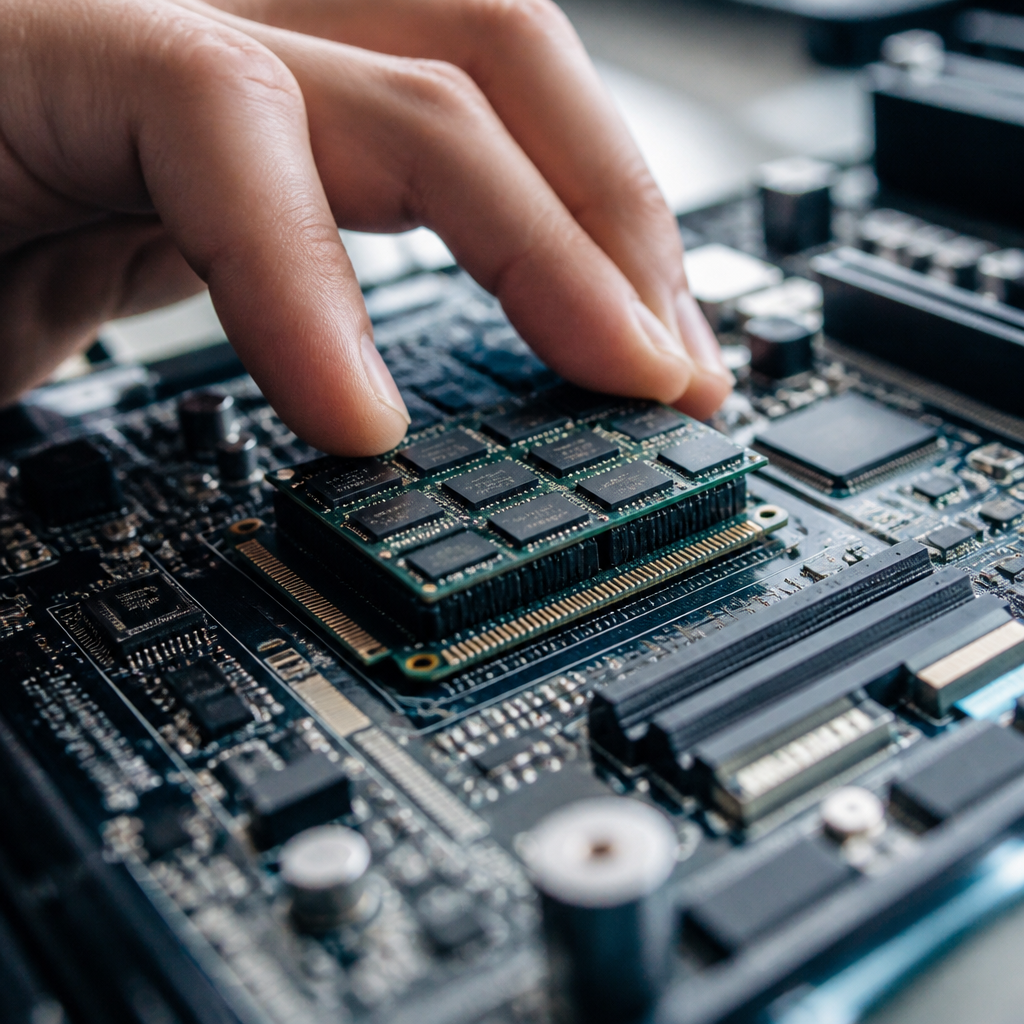
In-memory computing is moving from a specialist semiconductor concept to a central question for AI infrastructure: can startups reduce the cost, latency, and energy lost when data shuttles constantly between memory and processors? In simple terms, in-memory computing shifts part of computation closer to where data is stored, reducing the data-movement bottleneck that limits modern AI systems. For startups working in semiconductors and compute, that promise matters because training and inference workloads increasingly spend more power on moving bits than on arithmetic itself. I have seen this issue surface repeatedly in chip briefings, accelerator benchmarks, and customer evaluations: a design may advertise massive TOPS or TFLOPS, yet real application performance collapses when memory bandwidth, memory capacity, or interconnect efficiency becomes the constraint. That gap between theoretical compute and delivered system throughput is where in-memory approaches are trying to compete.
As a hub topic under semiconductors and compute, this subject connects several core themes: AI accelerators, high-bandwidth memory, near-memory processing, analog compute, chiplets, packaging, and the software stacks needed to make unfamiliar hardware usable. It also intersects with business reality. Startups do not win by inventing an elegant architecture alone; they need manufacturable devices, credible reliability data, a compiler toolchain, and a path into cloud, edge, or enterprise deployments. Understanding in-memory computing therefore requires both technical and commercial context. The key question is not whether moving compute toward memory is intellectually attractive; it clearly is. The real question is whether startups can beat conventional GPU roadmaps, survive long design cycles, and deliver enough software compatibility to persuade customers to adopt a new compute model for AI.
What in-memory computing means in AI systems
In-memory computing describes architectures that perform certain operations inside memory arrays or very close to them, instead of repeatedly fetching data into a separate logic core. The problem it targets is rooted in the traditional von Neumann architecture, where memory and compute are physically separated. Every matrix multiplication, attention step, vector search, or recommendation query requires operands to travel across buses and hierarchies of caches, DRAM, and interconnects. That travel adds latency and burns energy. Industry measurements vary by process node and memory type, but the established principle holds: a memory access often costs far more energy than a multiply-accumulate operation. For AI, especially transformer inference and embedding-heavy models, memory traffic can dominate total system cost.
There are several forms of in-memory computing. Digital near-memory processing adds lightweight compute units adjacent to SRAM or DRAM. Analog in-memory computing uses the physical properties of memory cells, often resistive RAM, phase-change memory, or SRAM arrays, to execute matrix-vector operations directly inside crossbar structures. Processing-in-memory, often abbreviated PIM, is the broader category that includes integrating compute functions into or alongside memory devices. Samsung and SK hynix have both discussed PIM concepts for high-bandwidth memory, while research groups at IBM, MIT, and others have demonstrated analog approaches for neural networks. Startups entering this space usually position themselves along a spectrum: some emphasize radical analog efficiency; others pitch a more incremental digital architecture that is easier to integrate into existing software and manufacturing flows.
Why the AI data-movement bottleneck keeps getting worse
The bottleneck is intensifying because model size, context length, and deployment volume are all expanding at once. Large language models require enormous parameter storage, fast access to key-value caches during inference, and sustained memory bandwidth during training. Recommendation systems and vector databases depend on fetching large embeddings with irregular access patterns. Computer vision at the edge must hit strict power envelopes while processing continuous sensor streams. In every case, arithmetic density improves more easily than memory movement economics. GPU vendors respond with wider memory buses, stacked HBM, larger on-chip SRAM, and advanced packaging, but those improvements are expensive and increasingly supply-constrained.
In practical benchmarking, I have found customers care less about peak tera-operations than about tokens per second per watt, tail latency at a given batch size, and total cost of ownership. An accelerator that advertises excellent raw throughput may fail if model weights cannot stay local, if KV cache spills into slower memory, or if host-device transfers dominate runtime. This is why semiconductors and compute cannot be analyzed only at the chip level. Packaging, HBM availability, PCIe or CXL connectivity, compiler graph optimization, and workload mapping all determine whether a startup architecture solves a real AI bottleneck or simply moves it elsewhere.
Where startups think they can win
Startups target in-memory computing because incumbents have structural constraints. Established GPU platforms are optimized around a mature software ecosystem and a general-purpose parallel compute model. That scale is a strength, but it can slow architectural departures. A startup can design specifically for sparse inference, low-bit matrix operations, database search, or edge AI and claim superior energy efficiency by minimizing data movement from the outset. Some companies also avoid the highest-risk frontier by focusing on narrower workloads where deterministic performance matters more than broad programmability, such as industrial vision, telecom signal processing, or retrieval-heavy enterprise inference.
The likely startup advantages fall into four categories: lower energy per inference, reduced memory bandwidth pressure, smaller system footprints, and differentiated economics in edge deployments where thermal limits are unforgiving. The challenge is that each claimed advantage must survive contact with manufacturing and software. Analog arrays can drift, require calibration, and complicate precision management. Custom memory macros may not port cleanly across foundries. DRAM-integrated logic faces thermal and process tradeoffs. Meanwhile, buyers expect support for PyTorch, ONNX, TensorFlow Lite, or standard compiler paths such as MLIR. A hardware breakthrough without an acceptable software abstraction rarely reaches production.
Technical approaches and tradeoffs across the market
Not all in-memory architectures solve the same problem, and comparing them requires precision. Digital SRAM-based compute typically offers better determinism and easier integration, but lower theoretical density than analog crossbars. Resistive memory approaches can deliver highly parallel multiply-accumulate behavior, but non-idealities such as device variability, noise, endurance limits, and ADC overhead can erode system-level gains. HBM-based PIM may fit data-center AI because it works near existing memory subsystems, yet it depends on packaging economics and standardization progress. Compute-near-memory designs using chiplets can be more manufacturable, but the interconnect fabric still matters.
| Approach | Main benefit | Primary limitation | Best-fit use case |
|---|---|---|---|
| SRAM compute | Low latency, digital reliability | Area cost, limited density | Edge inference, cache-heavy workloads |
| Analog crossbar | High parallelism, strong energy potential | Precision drift, calibration overhead | Matrix-heavy neural inference |
| HBM PIM | Uses high bandwidth near data | Packaging complexity, ecosystem maturity | Data-center acceleration |
| Chiplet near-memory | Flexible partitioning and scaling | Interconnect and software complexity | Custom AI appliances |
This comparison is why blanket claims about replacing GPUs should be treated cautiously. In-memory computing is most credible when tied to a narrow performance target, such as reducing attention memory traffic, accelerating vector similarity search, or improving joules per inference for a fixed model class. General-purpose dominance is harder. NVIDIA, AMD, Intel, and hyperscalers are already attacking memory bottlenecks with larger caches, HBM3 and HBM3E, system-level optimization, and specialized kernels. Startups need a large enough efficiency delta to offset adoption risk.
What determines whether a startup breaks through
Three filters decide the outcome: manufacturability, software usability, and customer fit. Manufacturability means acceptable yield, packaging access, qualification data, and a roadmap beyond a lab prototype. Semiconductor history is full of architectures that looked excellent in papers but failed under process variation or cost pressure. Software usability means developers can compile models, profile bottlenecks, quantize safely, and debug numerical issues without rebuilding their entire stack. Customer fit means the startup can identify workloads where its architecture changes unit economics enough to justify switching.
The strongest go-to-market pattern is usually not “we replace all GPUs,” but “we cut inference power or memory cost dramatically for this specific deployment.” For example, an edge analytics vendor may value fanless operation more than peak flexibility. A vector database provider may pay for lower latency per rack if memory-bound search improves measurably. Telecom and automotive buyers may prioritize deterministic performance and thermal efficiency. Startups that align architecture, compiler support, and reference designs around one such pain point have a far better chance than those selling an undifferentiated accelerator dream.
The broader semiconductors and compute roadmap
As a hub for semiconductors and compute, in-memory computing should be viewed alongside adjacent innovations rather than in isolation. HBM scaling, CXL-attached memory, chiplet packaging, silicon photonics interconnects, sparsity-aware accelerators, and domain-specific compilers are all part of the same systems story. In many deployments, the winning solution will not be pure in-memory compute but a hybrid design that combines conventional logic, larger local memory, and selective near-memory acceleration. That hybrid path is more believable because it matches how enterprise infrastructure evolves: incrementally, with software continuity and mixed hardware generations.
The bottom line is clear. Startups can break parts of the AI data-movement bottleneck, but only where their architecture delivers system-level gains that are measurable, repeatable, and easy to adopt. The opportunity is real because AI demand is stressing memory economics faster than conventional scaling can comfortably answer. The risk is equally real because semiconductors reward integration discipline, not just architectural novelty. If you evaluate this space, focus on delivered throughput per watt, memory behavior under realistic workloads, toolchain maturity, and deployment fit before headline compute claims. That lens will help you separate promising in-memory computing startups from presentations that merely describe the bottleneck without truly solving it.
Frequently Asked Questions
What is in-memory computing, and why does it matter for AI infrastructure?
In-memory computing is a hardware approach that performs at least part of a calculation closer to, or directly inside, the memory array where data is stored. In conventional systems, processors and memory are physically separate, so AI workloads spend a large amount of time and energy moving model weights, activations, and intermediate data back and forth. That repeated transfer creates the so-called data-movement bottleneck, which can limit performance even when the raw compute engine is very powerful.
For AI infrastructure, this matters because modern training and inference are increasingly constrained not just by the number of arithmetic operations, but by how efficiently systems can feed those operations with data. Large language models, recommendation systems, and computer vision pipelines all rely on moving massive volumes of information through memory hierarchies. If a startup can reduce that movement, it may lower latency, improve throughput, and cut energy use at the same time. That is why in-memory computing has moved from a niche semiconductor idea to a serious strategic topic for AI hardware, hyperscalers, and edge-device designers.
How does in-memory computing reduce the AI data-movement bottleneck?
The core idea is simple: if data does not have to travel as far, the system wastes less time and power. In traditional architectures, data is fetched from memory, sent to a compute unit for processing, and often written back again. AI workloads repeat this pattern constantly, especially in matrix multiplication and vector operations that dominate neural network execution. In-memory computing changes that flow by embedding certain operations nearer to the stored data, so fewer transfers are needed.
In practice, this can take several forms. Some designs perform analog or digital operations inside memory arrays, while others place compute elements very close to memory banks. The exact implementation varies by company and process technology, but the goal is the same: reduce memory bandwidth pressure, shorten data paths, and improve effective system efficiency. For AI, where moving data can consume more energy than the computation itself, that architectural shift can be meaningful. The result is not magic elimination of all bottlenecks, but a potentially important reduction in one of the biggest cost centers in modern AI hardware.
Why are startups, rather than only major chip companies, so active in in-memory computing?
Startups are active because in-memory computing represents an architectural inflection point, and those moments often create openings for new entrants. Large incumbent chipmakers have deep expertise, manufacturing relationships, and software ecosystems, but they also have large product lines and established roadmaps that can make radical change slower. A startup can focus narrowly on a single problem, such as memory-centric AI acceleration, and design its hardware, software stack, and go-to-market strategy around that opportunity from day one.
There is also a commercial reason. AI demand is expanding so quickly that customers are actively looking for alternatives to conventional accelerators, especially if those alternatives can deliver better performance per watt, lower operating cost, or advantages in edge deployment. Startups that can prove real gains in inference efficiency, model serving, or specialized training scenarios may find receptive buyers in data centers, enterprise AI, automotive systems, robotics, and industrial deployments. That said, being early is not enough. In semiconductors, technical promise must be matched by manufacturability, software compatibility, reliability, and the ability to scale from demo to production.
What are the biggest technical and business challenges facing in-memory computing startups?
The challenges are substantial. On the technical side, startups must show that their architecture works not only in theory, but across real AI models and production conditions. Depending on the design, they may face issues involving precision, noise, thermal behavior, variability, endurance, and integration with standard digital logic. AI customers also care about programmability, toolchains, model portability, and support for mainstream frameworks. A hardware breakthrough that is difficult for developers to adopt can struggle commercially, no matter how elegant the underlying engineering may be.
On the business side, semiconductor execution is expensive and unforgiving. Tape-outs, packaging, validation, and system integration require major capital and long timelines. Startups must build credibility with foundries, secure strategic partners, and often educate the market while simultaneously competing with well-funded incumbents. They also need a clear beachhead use case. A general claim that data movement is inefficient is not enough; buyers want measurable improvements in total cost of ownership, latency, power draw, rack density, or edge-device battery life. The winners will likely be the companies that pair a differentiated architecture with a practical path to deployment and a software experience customers can actually use.
Can in-memory computing startups realistically break the AI data-movement bottleneck, or is the promise overstated?
The most realistic answer is that they may not eliminate the bottleneck entirely, but they can meaningfully reduce it in the right workloads. AI systems are complex, and no single architectural change solves every performance problem. Networking, storage, interconnects, model design, compilation, and memory hierarchy all affect end-to-end results. However, because data movement is such a fundamental source of inefficiency, even partial reductions can have outsized impact. If a startup can cut memory traffic for key tensor operations, improve energy efficiency, and maintain acceptable accuracy and software compatibility, that can translate into real competitive value.
Whether the promise is overstated depends on execution and claims. The strongest companies will be the ones that present clear benchmarks, production-relevant comparisons, and honest tradeoffs. Some applications, such as edge inference or highly repetitive matrix-heavy workloads, may benefit sooner than broad general-purpose training. Others may require hybrid architectures where in-memory techniques complement, rather than replace, standard GPUs or accelerators. So yes, startups can help break the data-movement bottleneck, but likely as part of a broader evolution in AI hardware rather than through a single sweeping replacement of existing compute platforms.