Lam Research sits at the center of semiconductor manufacturing, supplying the wafer fabrication equipment and process expertise that allow chipmakers to build smaller, faster, and more power-efficient devices at scale. In the Company Spotlights category, a Movers and Shakers hub article must do more than profile a single business; it needs to explain why the company matters, where it fits in the value chain, and how its decisions influence suppliers, foundries, memory makers, and the broader technology economy. Lam Research deserves that treatment because its tools are embedded in many of the most demanding steps of modern chip production, especially etch, deposition, and wafer clean.
In practical terms, Lam Research is one of the companies that make advanced semiconductor manufacturing possible. Chip design firms may create architectures, and foundries may run fabs, but equipment companies translate process recipes into repeatable physical results on silicon wafers. Lam’s systems help carve microscopic features, deposit precisely controlled films, remove unwanted materials, and maintain yield across high-volume production lines. Those capabilities are essential as the industry pushes into gate-all-around transistors, 3D NAND with hundreds of layers, advanced packaging, and process nodes measured in single-digit nanometers.
I have worked with semiconductor industry content and vendor positioning long enough to know that equipment firms are often underestimated by general business readers. They do not have the consumer visibility of Apple, NVIDIA, or TSMC, yet they are foundational to all of them. Understanding Lam Research means understanding a key layer of the semiconductor ecosystem: the firms that enable process integration, device scaling, and manufacturing economics. For readers exploring Movers and Shakers, this article functions as a hub by mapping Lam’s technologies, competitive position, customer base, strategic risks, and the adjacent topics worth following across the semiconductor equipment landscape.
What Lam Research Does and Why Its Tools Matter
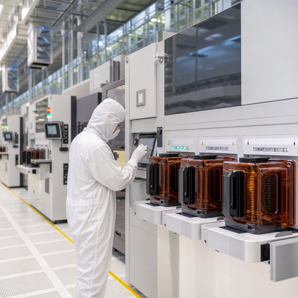
Lam Research is best known for wafer fabrication equipment used in front-end semiconductor manufacturing. Its core strengths are plasma etch, thin-film deposition, and wafer cleaning, with complementary software and services that help fabs manage process control and equipment productivity. These are not peripheral tasks. In an advanced logic or memory flow, etch and deposition happen repeatedly, often with atomic-level tolerances. If those steps drift, yields fall, defects rise, and the economics of the fab deteriorate quickly.
Etch systems remove material with extreme precision. For example, when a memory maker builds 3D NAND, it stacks layers and then etches deep, high-aspect-ratio channels through those layers. That is technically difficult because the profile must stay uniform from top to bottom without damaging surrounding structures. Deposition systems, by contrast, add films that serve as conductors, insulators, or barrier materials. Clean systems remove contaminants and residues that can interfere with downstream steps. Lam has built a portfolio around these critical operations, making it particularly strong in the process-intensive segments where scaling challenges are steepest.
This matters because modern semiconductor progress is no longer driven by lithography alone. Extreme ultraviolet lithography gets much of the attention, and rightly so, but pattern transfer, selective material removal, film conformity, and post-process cleanliness often determine whether a design can be manufactured reliably. That is where Lam Research creates value. The company helps customers convert design ambition into manufacturable process windows, which is why major foundries and memory producers treat equipment partners as strategic collaborators rather than interchangeable vendors.
Lam Research in the Semiconductor Value Chain
Within the semiconductor value chain, Lam Research operates upstream of chip production but downstream of materials science and subsystem suppliers. It purchases components such as RF power systems, vacuum hardware, robotics, sensors, and specialty materials, then integrates them into capital equipment installed in customer fabs. Its direct customers are typically integrated device manufacturers and foundries, including major memory companies and leading-edge logic producers. Revenue is shaped by wafer fab equipment spending cycles, technology migrations, and service demand from the installed base.
The company’s position is easiest to understand by comparing it with neighboring categories. Design software companies like Synopsys and Cadence define how chips are architected. Lithography specialist ASML prints patterns. Process control leaders such as KLA inspect and measure. Applied Materials spans several equipment categories. Lam Research stands out for its deep specialization in the fabrication steps that physically sculpt and prepare structures on the wafer. In industry conversations, that gives Lam influence well beyond its brand visibility because process bottlenecks in etch or deposition can hold back entire node transitions.
| Value Chain Area | Primary Role | Example Companies | Why Lam Research Matters |
|---|---|---|---|
| Chip Design | Create architectures and layouts | NVIDIA, AMD, Qualcomm | Designs depend on process capabilities Lam helps enable |
| Design Software | Electronic design automation | Synopsys, Cadence | Manufacturing rules reflect etch and deposition realities |
| Lithography | Pattern wafer features | ASML | Patterns must be transferred accurately through etch steps |
| Process Control | Inspection and metrology | KLA | Measures the quality of structures created with Lam tools |
| Wafer Fab Equipment | Etch, deposition, clean | Lam Research, Applied Materials | Core manufacturing steps for logic and memory devices |
| Chip Manufacturing | Run fabs at scale | TSMC, Samsung, Micron | Customers rely on Lam for yield, throughput, and process repeatability |
For a Company Spotlights hub, that ecosystem view is important because Lam Research should not be analyzed in isolation. It is a bellwether for capital intensity in semiconductors, for memory spending recoveries, and for the engineering complexity of advanced nodes. When Lam reports strong demand, it often signals confidence in future fab buildouts and technology roadmaps across the industry.
Core Technologies, Competitive Strengths, and Real-World Impact
Lam Research has built durable competitive advantages in areas where process difficulty acts as a barrier to entry. Plasma etch is one of them. In advanced memory and logic manufacturing, etch performance is not simply about removing material; it is about selectivity, profile control, uniformity, damage reduction, and integration with adjacent process steps. A tool that performs well in one layer but introduces downstream defectivity can fail commercially. Lam’s long history in conductor etch, dielectric etch, and high-aspect-ratio applications has made it especially relevant for 3D structures.
Deposition is another major pillar. Semiconductor films must often be deposited with angstrom-level control, excellent conformality, and repeatable material properties across the entire wafer and across chambers in high-volume manufacturing. Lam’s deposition portfolio supports a range of applications, including films used in transistor structures, interconnects, and memory architectures. In practice, fabs do not buy these tools just for headline specifications. They buy them because stable deposition can improve yield learning, shorten ramp times, and reduce cost per wafer over years of production.
Service and installed-base support are equally important. Once a system is qualified in a fab, uptime, spare parts availability, chamber matching, and field engineering responsiveness become central to the customer relationship. I have seen repeatedly that in semiconductor equipment, the sale is only the beginning. The long-term value often comes from process upgrades, maintenance contracts, software optimization, and productivity improvements that extend the usefulness of installed tools. Lam benefits from that model because recurring service revenue can cushion the swings of capital spending cycles.
Real-world impact is most visible in memory. NAND flash scaling has depended heavily on 3D architectures, which require repeated deposition and difficult etch steps through stacked layers. DRAM continues to demand tighter patterning and material control. Lam’s tools have been deeply connected to these transitions. In logic, the move toward FinFETs and then gate-all-around structures increases structural complexity and raises the stakes for precise materials engineering. As architectures become more three-dimensional, Lam’s expertise becomes more strategically valuable.
Business Strategy, Industry Cycles, and What to Watch Next
Lam Research operates in a cyclical industry, so strategy matters as much as technology. Demand is influenced by memory pricing, foundry utilization, geopolitical restrictions, and multiyear fab investment plans. The company must balance near-term revenue volatility with sustained research and development spending, because customers expect roadmaps that align with future device structures, not just current production needs. A weak spending year does not remove the need to prepare for the next node transition.
One major strategic theme is geographic diversification. Semiconductor manufacturing is expanding in the United States, Europe, Taiwan, South Korea, Japan, and parts of Southeast Asia, supported in some regions by industrial policy such as the U.S. CHIPS and Science Act and the European Chips Act. For Lam Research, regional fab expansion creates opportunity, but it also adds complexity in service logistics, local talent, supplier resilience, and compliance. Export controls, especially those affecting advanced manufacturing technology shipments to China, are a material variable for the entire equipment sector.
Another theme is the shift from pure scaling to system-level efficiency. Advanced packaging, heterogeneous integration, and AI-driven compute demand are reshaping where semiconductor value is created. While Lam is most associated with front-end wafer processing, the broader investment environment is being pulled by data center accelerators, high-bandwidth memory, and power efficiency requirements. Readers following Movers and Shakers should watch how Lam aligns its portfolio with AI infrastructure demand, memory recoveries, and increasingly complex device integration.
The clearest takeaway is that Lam Research is not just an equipment vendor; it is an enabler of semiconductor progress and a reliable signal of where manufacturing innovation is heading. Its strength in etch, deposition, and clean positions it close to the hardest technical problems in modern chip production, and that proximity gives the company lasting strategic relevance. For anyone tracking Company Spotlights and the semiconductor industry’s Movers and Shakers, Lam offers a textbook case of how specialized engineering capability can shape global technology outcomes.
As this hub article shows, the right way to evaluate Lam Research is through its role in the value chain, the precision of its core processes, the durability of its customer relationships, and the external forces that influence fab spending. Follow those factors and you can better understand not only Lam’s trajectory, but also the direction of memory, logic, AI hardware, and next-generation manufacturing. Use this page as your starting point, then explore related company profiles and equipment deep dives to build a fuller view of the semiconductor ecosystem.
Frequently Asked Questions
1. What does Lam Research do, and why is it so important to the semiconductor industry?
Lam Research is one of the core equipment suppliers that make advanced chip production possible. The company designs and manufactures wafer fabrication equipment used in critical semiconductor processes such as etching, deposition, cleaning, and wafer packaging. These are not peripheral steps; they are central to how integrated circuits are physically built layer by layer on silicon wafers. Without highly precise tools from companies like Lam Research, chipmakers would struggle to produce modern processors, memory chips, and specialized devices with the speed, yield, and consistency the market demands.
Its importance comes from where it sits in the semiconductor value chain. Lam Research operates upstream of the companies most consumers recognize, such as logic foundries, memory manufacturers, and integrated device makers. When those customers pursue smaller process nodes, denser memory architectures, or more advanced packaging methods, they rely on Lam’s process technologies to translate design ambitions into manufacturable reality. In other words, Lam does not simply sell machines; it provides process capability that directly affects how efficiently the world can produce smaller, faster, and more power-efficient chips at scale.
That role gives the company broader influence than a standard industrial supplier. Decisions Lam makes around product development, service support, and technology focus can shape production timelines, capital spending patterns, and competitive positioning across the semiconductor ecosystem. Its work matters to suppliers providing components, foundries building cutting-edge logic chips, memory makers scaling NAND and DRAM, and downstream technology companies waiting on more capable semiconductors. That is why Lam Research is often viewed not just as an equipment maker, but as an enabler of the industry’s next generation.
2. Where does Lam Research fit in the semiconductor value chain?
Lam Research occupies a critical position in the semiconductor manufacturing equipment segment, which sits between chip design and high-volume semiconductor production. Chip designers create architectures and circuit layouts, but those designs only become real products when manufacturers can reliably pattern, etch, deposit, clean, and package materials on wafers with atomic-scale precision. Lam supplies the tools and process expertise that support several of these fabrication steps, making it an essential partner to the companies that actually manufacture semiconductors.
In practical terms, Lam works closely with foundries, memory manufacturers, and integrated device manufacturers to help them solve production challenges. A foundry building advanced logic chips may depend on Lam’s etch and deposition systems to create increasingly complex transistor structures. A memory maker scaling 3D NAND may need Lam’s equipment to handle deep, high-aspect-ratio structures with extreme uniformity. Packaging and interconnect innovations may also involve Lam technologies that support better performance, lower power consumption, and higher device density.
This position gives Lam a unique view across multiple industry layers. It is not limited to one product category or one end market. Instead, it supports the manufacturing backbone behind smartphones, data centers, automotive electronics, AI accelerators, industrial systems, and consumer devices. Because it works so close to the production floor, Lam often becomes a strategic collaborator rather than a simple vendor. Its engineers and process specialists frequently help customers optimize yield, improve throughput, and shorten the path from technology development to commercial manufacturing. That value-chain role is one reason Lam Research carries such weight in discussions about semiconductor competitiveness and innovation.
3. How does Lam Research help chipmakers produce smaller, faster, and more power-efficient devices?
Lam Research helps chipmakers achieve better device performance by enabling more precise and repeatable manufacturing at extremely small scales. As semiconductor structures become more complex, the tolerances involved become extraordinarily tight. Tiny variations in etch depth, film thickness, material integrity, or particle contamination can affect yield and performance. Lam’s equipment is designed to manage those variables with a high degree of control, allowing customers to build intricate device architectures that support higher speed, lower power consumption, and improved transistor density.
One major area is etching, where selected material must be removed from a wafer with exceptional accuracy. Advanced chips often require complex three-dimensional structures, and creating those structures demands tools that can etch deep, narrow features without damaging adjacent layers. Lam’s capabilities in this area are especially important for both leading-edge logic and memory production. Deposition is another key contribution. Thin films must be laid down with exact composition and uniformity, because these films form part of the electrical and structural foundations of semiconductor devices. Cleaning technologies are just as important, since contamination can ruin high-value wafers and reduce production yields.
Beyond the equipment itself, Lam contributes process knowledge that helps manufacturers move from lab-scale innovation to stable, high-volume output. That means improving throughput, reducing defects, and making complex manufacturing steps economically viable. This combination of hardware, software, and process expertise is what allows chipmakers to keep shrinking features while increasing performance per watt. In a market where progress depends on turning physical complexity into scalable production, Lam Research plays a direct role in helping the industry push beyond previous technical limits.
4. Why do Lam Research’s decisions affect foundries, memory makers, suppliers, and the broader technology market?
Lam Research has influence well beyond its own operations because semiconductor manufacturing is deeply interconnected. When Lam develops a new process capability, adjusts its production roadmap, or prioritizes certain technology areas, those choices can ripple through the entire ecosystem. Foundries may align capacity expansion plans around the availability of new equipment. Memory manufacturers may depend on Lam’s process advances to improve layer counts, yields, or cost efficiency. Suppliers that provide subsystems, materials, and precision components may scale production in response to Lam’s demand patterns. Even downstream technology companies can feel the impact if equipment innovation helps accelerate chip availability or improve semiconductor performance.
This influence is especially visible during major industry transitions. As manufacturers move to more advanced logic nodes, stack more layers in memory, or invest in new packaging techniques, equipment readiness becomes a strategic issue. If the right tools are available with strong process support, customers can move faster and with lower risk. If bottlenecks emerge, they can delay product ramps, constrain supply, or increase manufacturing costs. Because Lam serves many of the world’s most important semiconductor producers, its execution can affect broader trends in capital investment, production efficiency, and technology adoption.
There is also a strategic dimension tied to geography, supply chain resilience, and industrial policy. Semiconductor manufacturing has become a national and economic priority in many regions, and companies like Lam are central to that conversation. Their ability to support advanced manufacturing capacity influences competitiveness, regional expansion efforts, and the practical pace of industry growth. That is why Lam Research is often discussed not only as a company with strong products, but as one whose decisions can shape the operating environment for a wide range of players across the semiconductor and technology landscape.
5. What makes Lam Research a noteworthy company in a Movers and Shakers or Company Spotlights article?
Lam Research stands out because it represents the kind of company that quietly drives major technological progress from behind the scenes. It may not have the same consumer visibility as a major chip brand, but its contribution is foundational. A strong Company Spotlights or Movers and Shakers article should highlight that distinction: Lam is not simply participating in semiconductor growth, it is helping make that growth technically possible. Its equipment and process expertise support some of the most difficult manufacturing steps in the industry, which means its relevance extends far beyond its own balance sheet or product catalog.
The company is also noteworthy because it sits at the intersection of several defining semiconductor themes: advanced scaling, memory innovation, manufacturing efficiency, capital intensity, and supply chain strategy. That makes Lam a useful lens for understanding how the industry actually functions. By examining Lam, readers can better understand how foundries bring advanced chips to market, how memory producers increase density, why production yield matters so much, and how upstream equipment makers influence the pace of innovation. In that sense, Lam is both a subject and a gateway to understanding the broader semiconductor ecosystem.
For a Movers and Shakers hub article, that broader relevance is essential. The goal is not just to explain what Lam Research sells, but why its role matters to investors, industry observers, technology leaders, and anyone trying to understand how modern electronics are made. Lam’s importance comes from its leverage within the value chain. When it innovates, customers can manufacture more capable chips. When it executes well, the industry gains efficiency and scale. When it faces challenges, those effects can be felt across production schedules and technology roadmaps. That combination of technical depth, ecosystem impact, and strategic significance is exactly what makes Lam Research a compelling spotlight company.