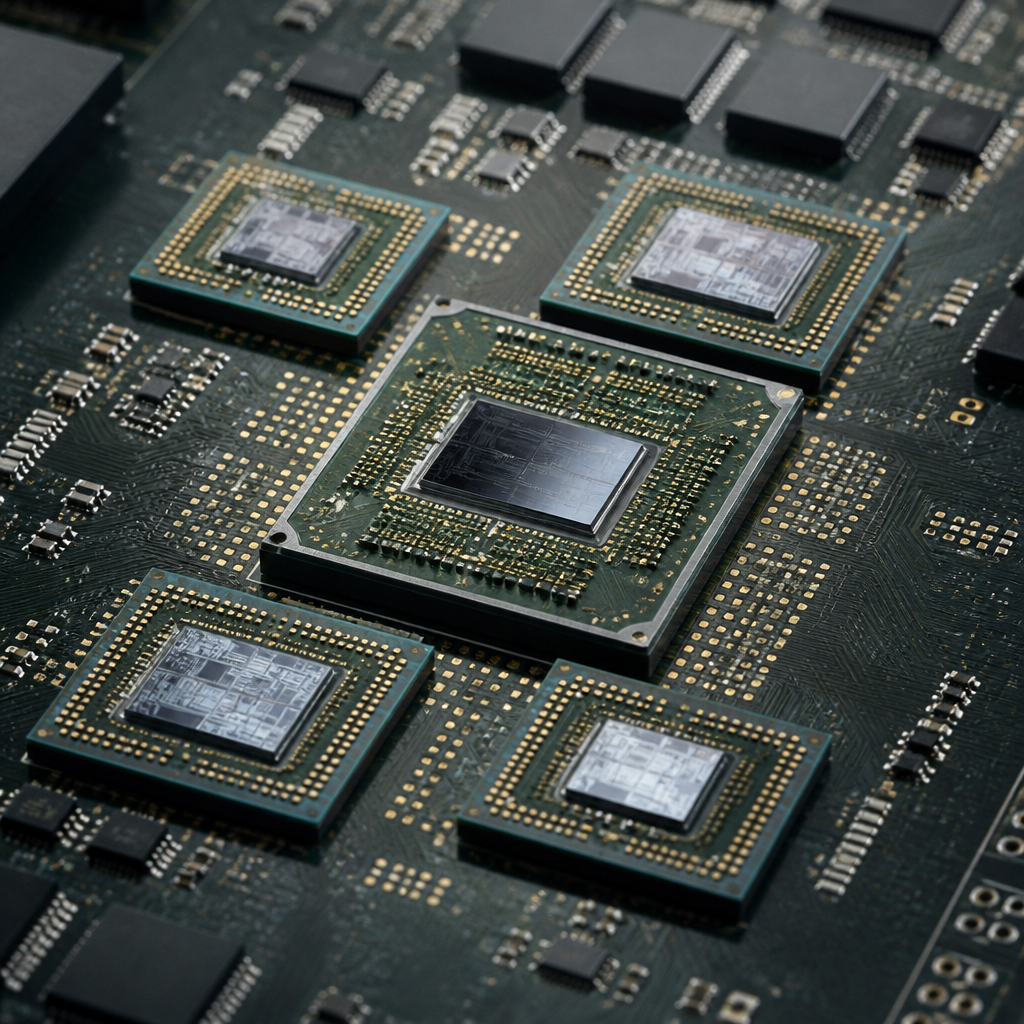
Chiplets are small, specialized silicon dies combined in a single package to create a processor, and they are rapidly changing how advanced chips are designed, manufactured, and scaled. Instead of building one large monolithic die that contains CPU cores, cache, graphics, memory controllers, and input-output logic, engineers split those functions into modular blocks. In practice, this means a processor can mix compute tiles built on a leading-edge process with I/O dies, accelerators, or analog components built on older, cheaper nodes. I have worked on product positioning around semiconductor roadmaps, and the appeal of chiplets is straightforward: they reduce risk, improve yield, and give architects more flexibility than a single giant slab of silicon.
Understanding chiplets starts with three related terms. A die is one piece of silicon cut from a wafer. Packaging is the method used to connect one or more dies to each other and to the outside world. Advanced packaging includes technologies such as 2.5D interposers, fan-out redistribution layers, and 3D stacking that provide high-bandwidth, low-latency links between dies. A chiplet is a functional die designed to work as part of a larger system-in-package. That distinction matters because not every multi-die product is modular in the same way. True chiplet design treats dies as reusable building blocks with defined interfaces, power delivery assumptions, and test flows.
Why this matters goes far beyond clever engineering. Semiconductor economics have changed. As process nodes shrink from 7 nanometer to 5 nanometer to 3 nanometer classes, wafer costs rise sharply, defect sensitivity increases, and development expenses climb into the hundreds of millions of dollars for high-volume products. Large monolithic dies become harder to yield and harder to update. Chiplets offer a way to keep performance moving while managing cost and complexity. They also open the door to a more diverse compute landscape, where CPUs, GPUs, AI accelerators, networking blocks, and memory can be assembled in combinations that fit specific markets, from cloud servers to laptops to automotive systems.
How chiplet architecture works in real processors
Chiplet architecture separates functions that do not scale equally with process technology. CPU cores and dense SRAM often benefit most from advanced nodes because they gain performance per watt and transistor density. I/O functions such as PCIe, DDR memory controllers, USB, or SerDes may see smaller benefits, so placing them on a mature node can save money without sacrificing system value. AMD demonstrated this clearly with its Zen 2 and later EPYC server processors, where multiple compute chiplets connect to a central I/O die. That design allowed AMD to use TSMC 7 nanometer for core complexes while keeping I/O on GlobalFoundries 12 nanometer, balancing cost, thermals, and manufacturing efficiency.
Intel has pursued a similar strategy with products that combine tiles using EMIB and Foveros packaging. In Meteor Lake, for example, compute, graphics, SoC, and I/O functions are partitioned across tiles from different process technologies and then assembled in one package. The principle is consistent across vendors: disaggregate the system into blocks that can be optimized independently. This modularity speeds product derivation. A company can reuse an I/O die across several processor tiers, pair different numbers of compute chiplets for scaling, or integrate a custom accelerator for a niche workload without redesigning the entire chip from scratch.
The package becomes part of the architecture, not just a protective shell. Interconnect choices determine bandwidth, latency, power efficiency, and software transparency. Infinity Fabric, Intel’s die-to-die links, TSMC CoWoS, and silicon interposer-based approaches all influence how closely multiple dies behave like a single chip. If interconnect latency is too high, memory access and cache coherency suffer. If power delivery is uneven, boosting behavior becomes unpredictable. For that reason, chiplet success depends on co-design across silicon, package, firmware, and platform. This is one reason advanced processors increasingly look like miniature systems assembled at the package level.
Why modular silicon improves cost, yield, and product strategy
The economic case for chiplets is best understood through yield. Defects occur randomly across a wafer. The larger the die, the greater the chance that one defect ruins it. Splitting a 600 square millimeter processor into smaller dies raises the probability that each die is good, and known-good dies can then be packaged together. That does not eliminate packaging cost or testing complexity, but it often creates a better total cost structure. In server markets, where average selling prices are high, even modest yield gains can translate into major margin improvements and faster supply ramp.
Chiplets also shorten development cycles through reuse. A validated I/O die can support multiple CPU generations. A base compute chiplet can appear in desktop, workstation, and cloud products with different package counts or cache add-ons. AMD’s 3D V-Cache is a useful example of modular enhancement: additional cache is stacked onto selected processor dies to increase gaming and technical computing performance without redesigning the entire product. This kind of targeted upgrade is strategically powerful because it turns packaging innovation into a product lever.
| Approach | Main advantage | Main limitation | Example |
|---|---|---|---|
| Monolithic die | Lowest on-die latency | Poor yield at large sizes | Traditional mobile SoCs |
| 2D multi-die package | Function partitioning | Package trace limits | Early multi-chip modules |
| 2.5D chiplets | High bandwidth between dies | Higher packaging cost | AI GPUs with HBM |
| 3D stacked chiplets | Shortest vertical links | Thermal management challenges | Cache-on-logic designs |
Product strategy changes as well. Instead of building separate monolithic dies for every segment, vendors can create families from a smaller menu of silicon building blocks. That supports faster response to market demand, tighter inventory control, and more tailored offerings. For startups, this can lower entry barriers in selected categories. A company developing a domain-specific accelerator might not need to build a full SoC; it can design one chiplet and integrate it beside standard host logic, assuming packaging partners and interface standards are available.
Key technologies enabling chiplets at scale
Chiplets only work when the package can deliver near-monolithic behavior. Several technologies make that possible. Silicon interposers provide dense wiring between dies, which is why they are common in high-bandwidth memory systems. Organic substrates are cheaper but offer lower routing density. Bridges such as Intel EMIB embed small silicon pieces inside the package to connect adjacent dies without a full interposer. Foveros and TSMC SoIC support vertical stacking, reducing distance and power per bit. Each option involves tradeoffs among cost, thermal performance, assembly complexity, and achievable bandwidth.
Standards are becoming equally important. The Universal Chiplet Interconnect Express, or UCIe, aims to define an open die-to-die interconnect so chiplets from different vendors can communicate more easily. The concept resembles what PCI Express did for add-in connectivity at the board level, but brought inside the package. Broad industry support matters because an open ecosystem could allow foundries, IP vendors, and system companies to mix reusable components. In reality, interoperability will still depend on validation, packaging rules, and software support, but common electrical and protocol assumptions reduce friction.
Testing and power delivery are often overlooked enablers. Every die must be tested before assembly as a known-good die, then validated again after packaging. Signal integrity across short, high-speed links must be maintained under thermal and voltage variation. Power management must coordinate multiple dies with different leakage characteristics and process nodes. In my experience, these details determine whether a chiplet roadmap scales smoothly or becomes an integration bottleneck. The glamorous part is modular design; the hard part is making packaging, thermals, firmware, and manufacturing all behave predictably at volume.
Where chiplets are headed in semiconductors and compute
Server processors and AI accelerators will continue leading chiplet adoption because they can justify advanced packaging costs with higher selling prices and intense demand for performance per watt. NVIDIA and AMD already rely on sophisticated package designs around HBM memory for data center products, and future accelerators will likely become even more modular as reticle limits constrain die size. Chiplets are a practical answer to those physical limits. They also support heterogeneous compute, where scalar CPU cores, matrix engines, networking, and secure enclaves sit in one package but are built and upgraded separately.
Client devices will adopt chiplets more selectively. Laptops and desktops benefit from modularity, but tight thermal envelopes and cost sensitivity mean only some segments will justify complex packaging. Mobile phones remain more monolithic today because board space, power efficiency, and package cost are unforgiving, though stacked memory and specialized companion dies already point toward more disaggregation over time. Automotive and edge systems are another important frontier because they often combine safety, AI inference, connectivity, and legacy interfaces that fit naturally into modular silicon strategies.
The broader implication for the Semiconductors and Compute landscape is that design leadership is shifting from transistor scaling alone to system integration. Winning companies will not just choose the best process node. They will choose what belongs on which node, what should be stacked, what can be reused, and which interconnect standard best supports future products. For readers exploring this hub topic, the next useful questions are practical ones: how advanced packaging affects startup opportunities, how AI accelerators differ from CPUs and GPUs, and how supply chains from TSMC, Intel Foundry, ASE, and Amkor shape what is commercially possible.
Chiplets explained simply means this: the future of processor design is modular, package-centric, and increasingly heterogeneous. By splitting a processor into smaller functional dies, chipmakers improve yield, control costs, and move faster across product generations. They can pair leading-edge compute with mature-node I/O, add memory or cache in three dimensions, and build more targeted products for cloud, client, automotive, and edge markets. That is why chiplets matter not as a niche packaging trick but as a structural change in semiconductor design.
The most important takeaway is that chiplets solve both an engineering problem and a business problem. Engineering teams gain flexibility to optimize each function on the right process and connect them with advanced packaging. Business teams gain reusable platforms, better supply resilience, and more ways to segment the market without funding a new monolithic die each time. There are tradeoffs, especially around thermal management, validation, and software tuning, but the direction is clear: modular silicon is becoming a core design pattern for modern compute.
If you follow technology innovation, startups, or infrastructure trends, chiplets are worth watching closely because they influence everything from AI servers to laptop roadmaps and semiconductor investment strategy. Use this hub as your starting point for deeper coverage across packaging, foundries, accelerators, memory, and processor architecture. The companies that master chiplet integration will shape the next decade of compute, so now is the right time to understand how modular silicon changes the rules.
Frequently Asked Questions
What is a chiplet, and how is it different from a traditional monolithic processor die?
A chiplet is a smaller, purpose-built silicon die that performs a specific function inside a larger processor package. Instead of placing every major subsystem—such as CPU cores, cache, graphics, memory controllers, and input-output logic—onto one large piece of silicon, chiplet-based design breaks those functions into modular blocks. Those blocks are then connected inside the same package using high-speed interconnects, advanced packaging, and carefully engineered signaling pathways so the finished product behaves like one processor from the system’s point of view.
That is fundamentally different from a monolithic die, where all functions are fabricated together on one large chip. Monolithic processors can deliver excellent integration, but they become increasingly difficult and expensive to manufacture as transistor densities rise and die sizes grow. A defect anywhere on a large monolithic die can ruin the entire chip, which hurts yield and raises cost. With chiplets, manufacturers can produce smaller dies more efficiently, test them individually, and combine only known-good components into a final package.
This modular approach also gives chip designers far more flexibility. A company can reuse the same I/O die across multiple products, pair different numbers of compute chiplets to target different performance tiers, or mix process nodes so the most performance-sensitive logic uses the latest manufacturing technology while less demanding functions stay on a more mature and cost-effective node. In short, chiplets turn processor design from a single giant silicon problem into a system-level integration problem, and that shift is a major reason they are reshaping modern semiconductor development.
Why are chiplets becoming so important in modern processor design?
Chiplets are becoming important because they solve several of the biggest economic and engineering problems facing advanced semiconductors. As process nodes become more expensive, producing one massive leading-edge die is no longer the best answer for every product. Very large dies are harder to manufacture, more vulnerable to defects, and more costly to scale. By dividing a processor into smaller functional dies, chipmakers can improve yields, lower waste, and make better use of expensive wafer capacity.
They also support a more practical path to performance growth. Not every part of a processor benefits equally from the newest node. High-performance CPU or GPU compute logic may need the transistor density and power efficiency of a leading-edge process, while analog circuitry, memory interfaces, and I/O often do not. Chiplets allow designers to place each function on the process technology that fits it best. That can improve overall cost efficiency without sacrificing competitiveness.
Another major reason is product agility. A modular architecture makes it easier to create multiple processors from a shared library of silicon building blocks. Instead of designing entirely separate chips for servers, desktops, and embedded systems, a company can combine similar chiplets in different package configurations. That shortens development cycles, spreads research and design costs across more products, and helps companies respond faster to market demands. In that sense, chiplets are not just a packaging trend—they are becoming a core business and engineering strategy for scaling processor families.
How do chiplets improve manufacturing efficiency and scalability?
Chiplets improve manufacturing efficiency primarily through better yield management. Smaller dies generally have a higher chance of being defect-free than large dies because any given manufacturing flaw affects less silicon area. In a monolithic design, one defect can render a very large and expensive chip unusable. In a chiplet design, the defective die can be discarded while other working dies from the same wafer remain useful. Over time, that translates into lower effective costs and better output from advanced fabrication lines.
They also improve scalability by letting chipmakers build bigger or more specialized processors without relying on a single enormous die. There are practical reticle limits in lithography, thermal concerns, and escalating complexity when trying to keep expanding monolithic silicon. Chiplets provide a way around those barriers. Designers can scale a product by adding more compute chiplets, larger cache dies, or dedicated accelerators in the same package, creating a broader range of processors from the same design ecosystem.
Equally important, chiplets support heterogeneous integration. A processor package can combine logic made by different fabrication processes and, in some cases, even from different foundries. That means manufacturers can choose the most sensible production path for each functional block rather than forcing all components onto one process technology. When paired with advanced packaging methods such as 2.5D interposers, organic substrates, or 3D stacking, chiplets create a more flexible and scalable platform for future processor designs. The result is a manufacturing model that is often more resilient, more economical, and better suited to the demands of modern high-performance computing.
Are there any drawbacks or technical challenges with chiplet-based processors?
Yes—chiplets solve many problems, but they also introduce important new challenges. The first is interconnect complexity. When functions that once lived on the same die are split across multiple dies, communication between them must cross package-level links rather than short on-die wires. Those links need to deliver extremely high bandwidth, low latency, strong power efficiency, and excellent reliability. Achieving that requires sophisticated packaging, signaling, and protocol design, and it can become a bottleneck if not done well.
Power delivery and thermal management are also more complicated. A multi-die package may contain chiplets with different power profiles, hotspots, and cooling requirements. Keeping those dies synchronized and efficiently powered while maintaining signal integrity is not trivial. Engineers must optimize placement, packaging materials, and interface design so the system performs like a cohesive processor rather than a collection of loosely connected parts.
Software and validation complexity can rise as well. Even if a chiplet-based processor appears unified to the operating system, the underlying architecture may have subtle differences in latency, cache behavior, memory access, or accelerator integration. Testing all of those interactions is demanding. Standardization is another ongoing issue. The industry is moving toward more open chiplet interconnect ecosystems, but broad interoperability across vendors is still developing. So while chiplets offer major advantages, they shift the challenge from simply designing a larger die to mastering advanced integration across silicon, packaging, firmware, and platform architecture.
What does the future of chiplets look like for CPUs, GPUs, and specialized accelerators?
The future of chiplets looks extremely strong because they align well with where the semiconductor industry is heading: more specialization, more heterogeneous computing, and more pressure to improve performance without letting costs spiral out of control. For CPUs, chiplets will likely continue enabling scalable product families, where manufacturers can mix and match compute tiles, cache dies, and I/O components to serve everything from laptops to data center servers. That makes it easier to tailor performance, core counts, and platform features without redesigning an entire processor from scratch.
For GPUs and AI accelerators, chiplets are especially promising because these devices demand massive parallelism, huge memory bandwidth, and fast data movement. Rather than building one giant die that is difficult to manufacture and expensive to yield, designers can distribute compute across multiple tiles and connect them with very high-speed package interconnects. This can support larger effective processors and more modular upgrade paths for different market segments. It also opens the door to combining general-purpose compute with dedicated AI, networking, security, or memory-expansion chiplets in one tightly integrated package.
Looking further ahead, chiplets may help create a more modular semiconductor ecosystem overall. As packaging standards and interconnect technologies mature, the industry could move toward more reusable silicon components and even broader multi-vendor integration. That would not mean processors become simple plug-and-play assemblies overnight, but it would represent a major shift in how advanced chips are architected and commercialized. In practical terms, chiplets are likely to remain one of the most important design strategies for extending performance, improving manufacturing economics, and enabling the next generation of high-performance and specialized computing systems.