William Shockley’s move to Mountain View in 1956 marked the disputed starting point of Silicon Valley semiconductors, linking Nobel-level transistor science with a management culture that pushed brilliant engineers away and, in doing so, seeded an entire regional industry. To understand why this moment matters, it helps to define the core terms. A semiconductor is a material, usually silicon or germanium in the 1950s context, whose electrical conductivity can be controlled through impurities, electric fields, and layered structures. The transistor is a semiconductor device that amplifies or switches electrical signals, replacing bulkier vacuum tubes in radios, computers, missile guidance systems, and later nearly every electronic product. Silicon Valley semiconductors refers not just to chips made in Northern California, but to the tightly connected network of laboratories, suppliers, venture capital, universities, and spinout companies that emerged from early device work on the San Francisco Peninsula.
I have worked through archival timelines, oral histories, and company records on this period, and one fact stands out: the origin story is not clean. Shockley was unquestionably a scientific giant. At Bell Labs, he helped create the transistor and shared the 1956 Nobel Prize in Physics with John Bardeen and Walter Brattain. Yet the semiconductor roots of Mountain View are controversial because the same founder who brought world-class expertise to the region also created the conditions for rebellion. His company, Shockley Semiconductor Laboratory, attracted elite young physicists, chemists, and device engineers. Their departure in 1957 produced Fairchild Semiconductor, the company that became the training ground for Intel, AMD, National Semiconductor, and dozens of other firms. In other words, Shockley did not build Silicon Valley in the heroic, straightforward sense often suggested. He triggered it through a combination of technical ambition, strategic geography, and managerial failure.
As a hub page on semiconductor roots, this article maps the main themes readers need: why Mountain View was chosen, what Shockley was trying to invent, how his lab operated, why the so-called Traitorous Eight left, and how that breakaway created the commercial DNA of the modern chip industry. If you are exploring historical perspectives on electronics, startup formation, research culture, or the origins of venture-backed deep technology, this is the central story that connects them.
Why Shockley Chose Mountain View
Shockley did not place his laboratory in Mountain View by accident. He grew up partly in Palo Alto, and his mother lived in the area, so there was a personal pull toward the Santa Clara Valley. But location also made strategic sense. Stanford University, under Frederick Terman’s influence, was encouraging industry links, leasing land to technology firms, and helping transform defense-funded research into local enterprise. The region already had specialized machine shops, access to military electronics contracts, and a climate attractive to scientists relocating from the East Coast. Before integrated circuits defined the Valley, the area had a growing base in microwaves, vacuum tubes, instrumentation, and applied physics. Shockley recognized that advanced semiconductor work needed nearby talent and flexible suppliers, not just laboratory prestige.
His new operation was established as Shockley Semiconductor Laboratory, a division of Beckman Instruments. Arnold Beckman provided the corporate umbrella and capital. That backing mattered because semiconductors were not yet a proven standalone business. Device fabrication involved crystal growth, diffusion, contamination control, metallization, and packaging methods that were expensive, fragile, and difficult to scale. Locating in Mountain View gave Shockley room to build a specialized lab while recruiting aggressively from top schools and laboratories. It also planted semiconductor R&D next to an emerging university-industry corridor that would later define the Valley’s growth model.
What Shockley Wanted to Build
Many summaries say Shockley came west to make transistors, but that is too broad to explain the semiconductor roots of the region. He was focused on pushing beyond the early junction transistor toward more powerful and potentially manufacturable devices. One major concept was the four-layer diode, often called the Shockley diode, based on alternating p-type and n-type semiconductor regions. Shockley believed this switching device could outperform conventional transistor designs in some applications. The idea was not irrational; the 1950s were full of competing device architectures, and no one yet knew which structures would dominate military and commercial electronics.
The problem was execution. Manufacturing semiconductors in that era required extraordinary process discipline. Tiny variations in impurities, temperature, and surface contamination could ruin yields. Bell Labs had the benefit of a large institutional system with deep materials science capability. In Mountain View, Shockley had brilliant recruits, but he steered them toward projects many considered commercially premature. Some engineers wanted to make proven silicon transistors that customers would buy. Shockley repeatedly redirected effort toward his preferred concepts. In the lab histories I have reviewed, this mismatch between technical possibility and business practicality appears again and again. It is one reason the laboratory’s direct commercial output remained limited even though its talent density was exceptional.
The Laboratory Culture and Its Breakdown
Shockley’s reputation as a difficult manager is not a later exaggeration added for drama. Multiple accounts describe a culture of distrust, abrupt criticism, and erratic decision-making. He screened employees intensely, involved himself in personal matters, and became suspicious that staff members were undermining him. One frequently cited incident involved lie detector testing after he believed someone had caused deliberate harm in the lab. Whether every remembered detail is precise, the broad pattern is clear: morale deteriorated because highly trained specialists were not treated as trusted colleagues.
That matters historically because semiconductor innovation depends on coordinated expertise. Crystal growers, device physicists, metallurgists, chemists, and process engineers must share information rapidly. Fear slows problem solving. In a good fab culture, defects are surfaced early, experiments are documented, and disagreements are resolved through data. In Shockley’s lab, the management environment made ordinary technical debate feel risky. The result was not simply unhappiness. It was organizational paralysis at exactly the moment when silicon devices required disciplined iteration.
| Issue | At Shockley Semiconductor | At Fairchild Semiconductor |
|---|---|---|
| Leadership style | Centralized, suspicious, founder-driven | Collaborative, team-based, execution-focused |
| Product focus | Advanced but commercially uncertain devices | Planar silicon transistors and scalable production |
| Decision making | Frequent reversals and personal control | Faster engineering consensus tied to customers |
| Legacy | Talent concentration without market success | Template for Valley spinouts and chip scaling |
The Traitorous Eight and the Founding of Fairchild
The decisive break came in 1957, when eight key employees left Shockley Semiconductor Laboratory. They were Julius Blank, Victor Grinich, Jean Hoerni, Eugene Kleiner, Jay Last, Gordon Moore, Robert Noyce, and Sheldon Roberts. Shockley called them the Traitorous Eight, a label that endured, though history has judged their move as foundational rather than disloyal. They wanted competent management, a realistic product roadmap, and the freedom to build a company around silicon devices customers actually needed.
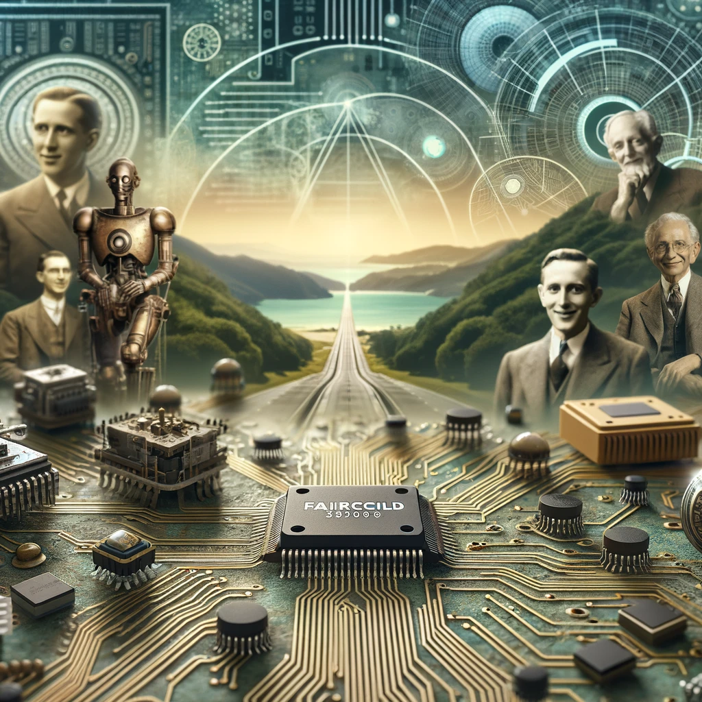
With investment arranged through Sherman Fairchild of Fairchild Camera and Instrument, the group founded Fairchild Semiconductor in Palo Alto. That financing structure became one of the Valley’s earliest examples of modern technology venture formation: a concentrated team, a parent investor, equity incentives, and a path to independent value creation. Fairchild quickly showed what Shockley’s original team could do under better leadership. Jean Hoerni developed the planar process, allowing silicon dioxide to protect transistor surfaces and making devices more reliable and manufacturable. Robert Noyce later applied planar principles to integrated circuits. Gordon Moore helped drive process and product discipline that would influence the industry for decades.
This is why any serious account of semiconductor roots must treat Shockley and Fairchild as one connected story. Shockley imported the talent and set the stage. Fairchild converted that talent into a scalable industrial model.
How Mountain View Helped Create Silicon Valley Semiconductors
Mountain View’s importance lies in clustering. Once Shockley recruited elite researchers to the Peninsula, the area gained credibility as a place where frontier electronics could be built outside the East Coast laboratory system. When Fairchild succeeded, employees learned not only device physics but also production control, sales to demanding customers, and the mechanics of starting new firms. This circulation of people became the Valley’s multiplier. Former Fairchild staff seeded Intel in 1968, and Fairchild alumni influenced National Semiconductor, Advanced Micro Devices, Intersil, LSI Logic, and many others. Venture investors increasingly understood that semiconductor startups could emerge from expert teams rather than giant incumbents alone.
The federal backdrop also mattered. Cold War defense spending supported demand for advanced electronics in radar, missiles, space systems, and communications. NASA and the Department of Defense purchased high-performance components even when yields were imperfect and costs were high. Stanford continued feeding talent and legitimacy into the ecosystem. By the 1960s, the region had acquired a self-reinforcing mix of research capacity, capital, production know-how, and ambitious labor mobility. That pattern began with semiconductors before it spread to computers and software.
The Controversy Around Shockley’s Legacy
Shockley remains controversial for two different reasons. First, his managerial role in the birth of Silicon Valley semiconductors is paradoxical. He was the catalyst, but not the builder of the enduring institutions that followed. Second, his later public advocacy of racist and eugenic theories rightly damaged his standing and complicates any celebratory narrative. Historical accuracy requires both points. His scientific contributions to transistor theory were major. His company’s direct business impact was small. His social views later in life were harmful and discrediting.
For readers using this sub-pillar hub to navigate semiconductor roots, the practical takeaway is simple: industry origins are often messy. Breakthrough regions are shaped by gifted individuals, failed companies, spinouts, university policy, defense money, and unresolved ethical contradictions. In Mountain View, Shockley’s arrival mattered because it concentrated expertise where a new industrial system could form. His failure to lead effectively mattered just as much, because it pushed that expertise into Fairchild, where the semiconductor business model truly took hold.
The beginning of Silicon Valley semiconductors was therefore not a single invention or a single founder’s triumph. It was a chain reaction: Bell Labs science, Beckman funding, Stanford proximity, Shockley’s ambition, employee revolt, Fairchild execution, and then waves of spinouts that defined the region. If you are exploring historical perspectives on technology, start here and follow the links across this semiconductor roots cluster to see how each company, process innovation, and founder dispute shaped the modern chip industry.
Frequently Asked Questions
Why is William Shockley’s move to Mountain View in 1956 often described as the beginning of Silicon Valley semiconductors?
William Shockley’s arrival in Mountain View in 1956 is often treated as a foundational moment because it connected world-class transistor research directly to a specific place that would soon become the center of the semiconductor industry. Shockley was already internationally famous as one of the key figures behind the invention of the transistor, work that helped earn the Nobel Prize in Physics. When he chose to establish Shockley Semiconductor Laboratory in Mountain View, he brought extraordinary scientific prestige, ambitious technical goals, and a new level of attention to the region. That decision mattered because it suggested that advanced electronics research and manufacturing did not have to remain concentrated in older East Coast industrial centers.
Just as important, Shockley’s company attracted a remarkable concentration of young scientific and engineering talent. Many of the people he recruited were highly trained physicists, chemists, and device engineers interested in pushing beyond existing vacuum tube technology into solid-state electronics. Although Shockley’s own firm struggled internally, the gathering of this talent in one place created the conditions for rapid industrial spillover. In that sense, the “beginning” was not simply the founding of one successful company. It was the beginning of a regional ecosystem built from expertise, risk-taking, technical ambition, and mobility between firms.
The moment is also described as “controversial” or “disputed” because historical beginnings are rarely neat. Some historians point to earlier electronics activity in Northern California, the role of Stanford University, or military and defense funding as equally essential roots of Silicon Valley. Those arguments are valid. Still, Shockley’s move remains symbolically powerful because it tied Nobel-level transistor science to Mountain View and directly triggered the chain of events that led to new companies, new manufacturing techniques, and a new business culture around semiconductors.
What exactly is a semiconductor, and why was it so important in the 1950s?
A semiconductor is a material whose ability to conduct electricity falls between that of a conductor, like copper, and an insulator, like glass. What makes semiconductors so valuable is that their conductivity can be deliberately controlled. In the 1950s, the most important semiconductor materials were silicon and germanium. Engineers learned that by introducing tiny amounts of other elements, called impurities or dopants, they could change how electrical charge moved through the material. This ability to engineer conductivity made semiconductors ideal for creating electronic components that could switch, amplify, and regulate current.
That mattered enormously because earlier electronic systems relied heavily on vacuum tubes, which were bulky, fragile, power-hungry, and generated significant heat. Transistors, built from semiconductor materials, promised smaller size, greater durability, lower power consumption, and higher reliability. These advantages opened the door to major advances in communications, computing, military electronics, instrumentation, and eventually consumer technology. In practical terms, semiconductors made it possible to imagine electronics becoming faster, cheaper, and far more compact.
In the 1950s, this was not just a scientific curiosity; it was a strategic technology with major commercial and national security implications. Companies and government agencies understood that whoever mastered semiconductor design and manufacturing would shape the future of modern electronics. That is one reason Shockley’s Mountain View venture drew so much attention. It sat at the intersection of cutting-edge physics, industrial production, and the emerging realization that semiconductors would become the foundation of a new technological era.
Why is William Shockley considered such a controversial figure in the history of Silicon Valley?
Shockley is controversial because his legacy combines undeniable scientific brilliance with deeply problematic leadership and later personal views. On the scientific side, he played a central role in the early development of the transistor, one of the most important inventions of the twentieth century. His reputation gave his Mountain View enterprise instant credibility and helped attract exceptional talent. Without that prestige, the early semiconductor scene in the region might have evolved more slowly or taken a different shape.
At the same time, Shockley’s management style became a serious obstacle inside his own company. He was widely regarded as distrustful, controlling, and difficult to work with. Rather than fostering collaboration, he often created an atmosphere of tension and instability. He was also known for pursuing technical directions that did not always align with what his team believed to be the most commercially practical path. The result was a paradox that sits at the heart of his story: the man who helped spark Silicon Valley’s semiconductor rise also drove away many of the people best positioned to build it.
His controversy extends beyond management. In later years, Shockley became infamous for promoting racist and discredited views about intelligence and heredity. Those views badly damaged his public standing and remain an inseparable part of any honest discussion of his life. As a result, Shockley is remembered not simply as a brilliant scientist or a failed executive, but as a deeply complicated and troubling figure whose influence on technology was profound even as his personal conduct and beliefs remain the subject of strong criticism.
How did Shockley’s management problems help lead to the rise of the broader Silicon Valley semiconductor industry?
One of the great ironies of Silicon Valley history is that Shockley’s managerial failures helped produce the very entrepreneurial network that made the region famous. The engineers and scientists he assembled in Mountain View were exceptionally talented, but many became frustrated by his leadership. They believed the company lacked a stable, effective environment for turning advanced semiconductor research into successful products. That frustration eventually pushed a key group of employees to leave and form their own company, Fairchild Semiconductor.
This breakaway event was hugely important. Fairchild became one of the most influential semiconductor firms in history, both technologically and organizationally. It helped advance silicon device production, manufacturing methods, and the commercial logic of the industry. Even more importantly, Fairchild became a training ground and launching pad for future founders, executives, and investors. Many later semiconductor and computer companies can trace part of their lineage back through Fairchild, creating what is often described as a corporate family tree running through Silicon Valley.
So while Shockley did not build the dominant company he imagined, his laboratory functioned as an unintended incubator. By concentrating talent and then failing to retain it, he accelerated the spread of expertise across multiple firms. That pattern—talented people leaving one company to start another, carrying ideas, techniques, and professional networks with them—became one of Silicon Valley’s defining traits. In that way, Shockley’s management problems were not just a footnote. They were part of the mechanism by which a single lab turned into a regional industry.
Why does this 1956 moment still matter when telling the story of Silicon Valley today?
The 1956 founding of Shockley Semiconductor Laboratory in Mountain View still matters because it captures several themes that continue to define Silicon Valley: the power of breakthrough science, the importance of place, the mobility of talent, and the unpredictable way innovation ecosystems actually form. It was a moment when advanced research stopped being only an academic or laboratory pursuit and began anchoring itself in a local industrial landscape. That shift helped transform Northern California from a region with technical promise into a region identified globally with high technology.
It also matters because it shows that innovation history is rarely a story of straightforward success. Shockley’s lab was not the final winner, yet it played a critical role in creating future winners. This is one of the most useful lessons from the episode. A failed or troubled company can still shape an industry if it gathers talent, develops expertise, and triggers the formation of new firms. Silicon Valley’s later culture of startups, spinouts, venture backing, and fast-moving technical communities has important roots in exactly this kind of fragmentation and recombination.
Finally, the moment matters because it reminds us that technological progress and human leadership are not the same thing. Shockley brought extraordinary scientific authority, but he did not create a healthy organizational culture. The region that emerged after him learned, in part through reaction against his example, that managing brilliant people well can be as important as having brilliant ideas in the first place. For readers trying to understand why Mountain View in 1956 remains so significant, that is the key point: it was not only the start of semiconductor activity in a place, but the start of a culture and industrial pattern that would reshape the modern world.