Lam Research sits at the center of modern chipmaking, supplying the wafer fabrication equipment that turns silicon into the memory and logic devices powering phones, cloud servers, electric vehicles, and artificial intelligence systems. For readers exploring company spotlights and diving deeper into corporate giants, Lam Research deserves close attention because it is not a consumer brand with flashy products; it is an industrial technology leader whose tools quietly shape the capabilities, cost, and yield of the semiconductor industry. In practical terms, Lam designs and services equipment used in critical manufacturing steps such as plasma etch, thin-film deposition, wafer cleaning, and process control, all of which determine whether a chip can be produced reliably at advanced nodes.
Understanding Lam Research also helps explain how the semiconductor value chain actually works. Chip designers like NVIDIA, AMD, Apple, and Qualcomm may capture headlines, but they depend on foundries and integrated device manufacturers that rely on highly specialized equipment vendors. In fabs I have studied and discussed with process engineers, the conversation repeatedly comes back to tool performance, uptime, defectivity, and process integration. That is where Lam has built its reputation. The company competes in segments where precision is measured at the atomic scale and where a small process improvement can save millions of dollars in wafer output. This article serves as a hub overview of Lam Research, its business model, competitive position, technology portfolio, and why its role matters across the broader landscape of corporate giants.
What Lam Research Does in Semiconductor Fabrication
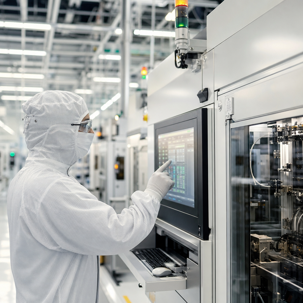
Lam Research is best known as a wafer fabrication equipment company focused on enabling semiconductor manufacturers to build increasingly complex devices. Its core systems are used after wafers enter the fab and before they emerge as finished chips. The company’s main categories include etch systems, deposition tools, and clean equipment. Etch removes selected material from the wafer to create patterns and structures. Deposition adds thin layers of insulating, conductive, or barrier materials. Clean systems remove particles, residues, and contaminants between process steps. These functions sound straightforward, but at advanced nodes they involve controlling plasma chemistry, film uniformity, profile shape, selectivity, and defect density with extraordinary precision.
Lam’s significance becomes clearer when you look at how chip structures have evolved. In planar transistor eras, process windows were difficult but broader. Today, FinFET, gate-all-around transistor architectures, 3D NAND memory stacks, and advanced DRAM capacitors require high aspect ratio structures, conformal films, and exact profile control. Lam has invested heavily in conductor etch and dielectric etch, as well as atomic layer deposition and specialty cleaning technologies tailored to these challenges. In memory manufacturing, especially NAND, Lam has long held strong positions because etching deep, narrow channels through many stacked layers is one of the defining process bottlenecks. When manufacturers increase layer counts, the need for sophisticated etch and deposition technology rises with them.
Customers include major foundries, memory makers, and logic manufacturers across Asia, the United States, and Europe. Taiwan Semiconductor Manufacturing Company, Samsung Electronics, SK hynix, Micron, and Intel all operate fabs where equipment in Lam’s categories is essential. The company generates revenue not only from new tool sales but also from spares, upgrades, service contracts, and installed base support. That recurring business matters because fabs run around the clock and cannot tolerate long equipment downtime. In equipment markets, service capability is often as strategically important as the original machine sale.
Technology Portfolio, Process Expertise, and Why It Matters
Lam Research has built its standing by focusing on process steps where manufacturing difficulty is high and customer switching costs are substantial. Etch remains a flagship area. Plasma etch systems remove material using reactive ions and gases under tightly controlled conditions. The technical challenge is not simply removing material; it is removing the right material at the right rate, in the right shape, without damaging nearby layers. For example, in 3D NAND manufacturing, etch tools must produce deep vertical channels through multilayer stacks while preserving profile integrity and minimizing bowing, twisting, and microloading effects. If that process drifts, device performance and yield suffer immediately.
Deposition is another essential domain. Thin films form the electrical and physical foundation of semiconductor devices, and Lam offers technologies for depositing materials with high uniformity and conformality. As structures become more three-dimensional, traditional film methods often struggle to coat every surface evenly. That is why atomic layer deposition and related advanced techniques have become more valuable. Clean technology, often underestimated by non-specialists, is equally vital. Even a tiny particle or post-etch residue can create killer defects, especially as line widths shrink and layer counts rise. I have seen engineers describe cleaning as one of the quiet determinants of yield because good cleaning prevents problems that are otherwise hard to diagnose later.
Lam also benefits from process integration expertise. Chipmakers do not buy isolated tools; they buy process capability that must fit within an entire manufacturing flow. A superior etch chamber means little if it creates downstream cleaning challenges or interacts poorly with deposition chemistry. This is why leading equipment companies invest in application labs, joint development work, and long customer qualification cycles. Lam’s value comes from combining hardware, software, consumables knowledge, and recipe tuning into a production-ready solution. That integration approach is a recurring theme among durable semiconductor equipment leaders.
Business Model, Financial Drivers, and Competitive Position
Lam Research operates in a capital equipment industry known for cyclicality, high barriers to entry, and concentrated customer relationships. Semiconductor manufacturers increase equipment spending during capacity expansions, technology migrations, and major memory upcycles, then reduce spending sharply during inventory corrections or weaker end demand. As a result, Lam’s revenue can swing with wafer fab equipment budgets. However, the company’s installed base business helps stabilize results. Once tools are in production, customers purchase replacement parts, chamber kits, software updates, and field support, creating a stream of recurring revenue tied to fab utilization.
Competition is intense and specialized. Applied Materials is broader across deposition, etch, and inspection-adjacent categories. Tokyo Electron is formidable in coat/develop, etch, deposition, and cleaning. KLA dominates process control and inspection rather than Lam’s core process tools. ASML, while not a direct rival in etch or clean, shapes fab investment through lithography spending. Lam’s competitive advantage comes from technical depth in selected categories, especially where process complexity supports premium performance and long qualification cycles. Once a tool wins a process of record in high-volume manufacturing, displacement is difficult because requalification carries cost, production risk, and timing pressure.
| Factor | Why It Matters for Lam Research | Real-World Impact |
|---|---|---|
| Installed base | Drives spares, service, and upgrade revenue | Supports cash flow even when new tool orders soften |
| Memory exposure | Lam is strong in NAND and DRAM process steps | Performance can improve sharply during memory capex recoveries |
| Process complexity | Advanced nodes require specialized etch and deposition | Raises customer dependence on proven tools and recipes |
| Customer concentration | A few large fabs drive much of industry spending | Winning or losing a major node transition has outsized effects |
Investors often watch gross margin, deferred revenue from services, free cash flow, and research spending to judge Lam’s quality. They also monitor foundry and memory capex guidance because that signals demand for future tool shipments. A useful way to think about Lam is that it sells picks and shovels into one of the most technically demanding industries in the world, but these are not commodity tools. They are deeply embedded production systems that influence customer yield, throughput, and cost per wafer.
Strategic Importance in the Global Semiconductor Ecosystem
Lam Research matters beyond its own income statement because semiconductor equipment companies sit upstream of nearly every digital industry. If fabs cannot acquire, install, and ramp advanced process tools, progress in smartphones, data centers, automotive electronics, industrial automation, and AI accelerators slows down. In recent years, geopolitical tension, export controls, and supply chain resilience have made equipment vendors more visible. Restrictions affecting advanced semiconductor manufacturing in China, for example, have altered demand patterns and forced equipment makers to navigate complex compliance requirements. For Lam, these policies can reshape near-term revenue mix, customer access, and competitive positioning in certain technology tiers.
The company is also relevant to sustainability and manufacturing efficiency discussions. Modern semiconductor fabs consume vast quantities of energy, water, specialty gases, and chemicals. Equipment vendors are under pressure to improve chamber efficiency, reduce waste, and support lower environmental impact per wafer. Lam has emphasized productivity, power efficiency, and resource management in its product development because customers increasingly measure suppliers on total cost of ownership, not just process performance. A tool that improves uptime and cuts consumable usage can provide meaningful savings over its service life.
For readers using this page as a hub within company spotlights, Lam Research offers a template for analyzing industrial technology giants. Look at where a company sits in the value chain, what technical bottlenecks it solves, how sticky its customer relationships are, and whether its products become more important as the underlying industry becomes more complex. By those standards, Lam stands out. Its fortunes are tied to semiconductor cycles, but its strategic role is anchored in the physics and economics of making advanced chips. To go deeper, explore related company profiles across equipment, lithography, foundry manufacturing, and chip design, then compare how each giant captures value from the same semiconductor ecosystem.
Lam Research shows why the most influential technology companies are not always the ones consumers recognize. Its tools enable the manufacturing steps that determine whether advanced semiconductors can be produced at scale, with acceptable yields and competitive costs. The company’s strength in etch, deposition, and clean systems places it close to the hardest problems in chip fabrication, especially as devices become more three-dimensional and process tolerances tighten. That position gives Lam strategic relevance with leading memory makers and foundries, while its service and installed base business provide resilience that pure equipment shipment figures can miss.
For anyone diving deeper into corporate giants, the main lesson is clear: follow the bottlenecks. Lam Research occupies manufacturing choke points where expertise, process integration, and customer trust matter enormously. Its future will still depend on semiconductor capital spending cycles, policy constraints, and competitive execution, but the underlying demand for precise fabrication technology is durable. Use this hub as a starting point for broader research into semiconductor equipment leaders, and continue with related company spotlight articles to understand how the industry’s most important firms connect across design, manufacturing, metrology, and supply chains.
Frequently Asked Questions
What does Lam Research actually do in the semiconductor industry?
Lam Research designs and supplies wafer fabrication equipment used by semiconductor manufacturers to build chips layer by layer on silicon wafers. In practical terms, the company provides highly specialized tools for critical production steps such as etching, deposition, cleaning, and related process technologies. These are not end-user products that consumers ever see on store shelves, but they are essential to making the memory and logic chips found in smartphones, laptops, cloud data centers, electric vehicles, industrial systems, and artificial intelligence infrastructure.
Lam’s importance comes from where it operates in the semiconductor value chain. Chipmakers rely on its systems to remove material with extreme precision, deposit ultra-thin films, and maintain the cleanliness and uniformity needed for advanced manufacturing. As chip architectures become more complex, including 3D structures and ever-smaller features, the performance of fabrication equipment becomes even more important. That places Lam Research in a strategic position: it helps enable the manufacturing breakthroughs that determine chip speed, power efficiency, density, and cost. In other words, Lam does not just support chipmaking; it helps define what is possible in modern semiconductor production.
Why is Lam Research considered so important if it is not a consumer-facing brand?
Lam Research matters because semiconductor progress depends as much on manufacturing capability as on chip design. A brilliant chip architecture means very little if it cannot be produced at scale with high yield, tight tolerances, and reasonable cost. Lam operates behind the scenes, but its equipment directly influences whether leading-edge chips can be manufactured efficiently and reliably. That makes the company a foundational player in the global technology ecosystem, even if its name is less familiar to the general public than the brands that sell finished devices.
This behind-the-scenes role is exactly why Lam deserves attention. The semiconductor industry is built on a network of deeply specialized firms, and equipment suppliers like Lam are among the most technically demanding businesses in that network. Their customers invest billions of dollars into fabrication plants, and every tool on the production floor must deliver precision, uptime, repeatability, and process control at an extraordinary level. When readers study Lam Research, they gain insight into the industrial backbone of digital life. The company illustrates how technological leadership often comes from firms that are invisible to consumers but indispensable to the performance, scalability, and economics of the devices and services people use every day.
How does Lam Research support the production of advanced memory and logic chips?
Lam Research plays a major role in both memory and logic manufacturing by supplying equipment used in some of the most difficult and valuable process steps. In memory, the shift toward increasingly dense structures, such as 3D NAND, has required manufacturers to etch deep, high-aspect-ratio features and deposit highly controlled films with remarkable uniformity. Lam’s tools are well suited to these challenges, which is one reason the company has long been closely associated with memory fabrication. As memory architectures continue to evolve, process precision becomes more critical, and that strengthens the need for advanced equipment solutions.
In logic chips, the demands are similarly intense. Modern processors and accelerators use increasingly complex transistor structures and multilayer interconnects, requiring precise pattern transfer, material engineering, and contamination control. Lam’s etch and deposition systems help manufacturers shape and build these structures at nanoscale dimensions. The company also supports yield improvement and process optimization, which are vital because even small defects can have major economic consequences at advanced nodes. By enabling high-performance, high-volume manufacturing across both memory and logic, Lam Research helps power everything from mobile devices to hyperscale computing and AI workloads.
What makes wafer fabrication equipment companies like Lam Research difficult to compete with?
The barriers to entry in wafer fabrication equipment are exceptionally high. First, the technology itself is extremely complex. Equipment must operate with extraordinary accuracy across countless process cycles while integrating chemistry, plasma physics, materials science, software, hardware engineering, vacuum systems, thermal control, and metrology. Second, semiconductor customers demand extensive validation before adopting any new tool because production interruptions or yield issues can be enormously expensive. That means established relationships, proven reliability, and deep process knowledge are as important as the machinery itself.
Lam Research also benefits from the long development cycles and close collaboration that define the industry. Tool suppliers often work directly with chipmakers to tailor equipment for emerging device architectures and manufacturing requirements. Over time, this creates a powerful ecosystem of expertise, service capability, installed base familiarity, and customer trust. Once a company becomes embedded in advanced production flows, replacing it is not simple. Competitors must match technical performance, global support, process know-how, and operational consistency at scale. That combination makes the sector highly defensible and helps explain why leading equipment companies such as Lam Research hold such influential positions in the semiconductor landscape.
Why should investors, business readers, and technology enthusiasts pay attention to Lam Research?
Lam Research offers a valuable lens into how the broader semiconductor industry functions and where it may be heading. For investors, the company can reflect capital spending trends among chipmakers, shifts in memory and logic demand, and the pace of technology transitions at major fabrication plants. Because semiconductor equipment sits upstream in the production cycle, firms like Lam are often watched closely as indicators of long-term industry confidence. Their performance can reveal how aggressively manufacturers are expanding capacity, adopting new process technologies, or preparing for future demand tied to AI, automotive electronics, cloud computing, and connected devices.
For business readers and technology enthusiasts, Lam is compelling because it represents the industrial foundation beneath digital innovation. Discussions about artificial intelligence, advanced computing, and electrification often focus on software platforms or consumer hardware, but none of those advances scale without sophisticated chip manufacturing. Lam Research helps make that scaling possible. Understanding the company means understanding a critical part of the real-world machinery that turns scientific progress into commercial technology. It is a reminder that the future of computing is shaped not only by the companies designing chips or selling devices, but also by the specialized firms whose tools quietly make the entire semiconductor ecosystem work.