Lam Research sits at the center of modern chipmaking because its equipment enables the precise etching, deposition, and cleaning steps that turn silicon wafers into advanced semiconductors. In the Company Spotlights landscape, Lam Research deserves a hub-level look because it represents more than one successful supplier; it shows how process equipment companies shape the roadmap for memory, logic, packaging, and ultimately the devices people use every day. When discussing Tech Innovators and Market Leaders, Lam Research is a defining case study: a company whose tools influence yield, transistor scaling, power efficiency, and factory economics across the global semiconductor industry.
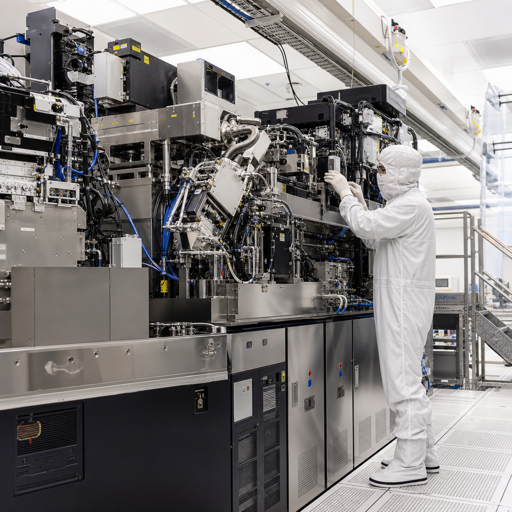
At its core, Lam Research designs wafer fabrication equipment and services used by integrated device manufacturers, foundries, and memory producers. Key terms matter here. Etch removes material with atomic-scale control. Deposition adds thin films that become insulating, conductive, or protective layers. Clean strips residues and contamination that can ruin device performance. Process control, productivity, and yield determine whether a fabrication plant can produce chips profitably at scale. I have worked with semiconductor content and manufacturing narratives long enough to know that nonengineers often focus on chip designers, while the real production bottleneck frequently sits inside these process steps. Lam matters because every improvement in its systems can ripple through billions of chips.
This article serves as a hub for understanding Tech Innovators and Market Leaders through Lam Research’s role in semiconductor production advances. It explains where the company fits in the value chain, what technologies define its importance, how it competes with peers, and why investors, supply chain analysts, engineers, and business readers keep tracking its moves. It also provides a practical framework for connecting Lam Research to adjacent company profiles across semiconductor equipment, materials, and manufacturing services. If you want to understand who enables chip progress beyond the headline brands, Lam Research is one of the essential names to study first.
Lam Research’s Position in the Semiconductor Value Chain
Lam Research operates in wafer fabrication equipment, the category of highly specialized systems used inside semiconductor fabs. Its customers include major memory producers such as Samsung Electronics, SK hynix, and Micron, along with logic and foundry leaders including TSMC and Intel. These manufacturers rely on process tools from companies like Lam, Applied Materials, ASML, KLA, and Tokyo Electron to convert design files into physical chips. In practical terms, Lam does not sell finished semiconductors to consumers. It sells the production capability that makes semiconductors possible.
The company’s importance becomes clearer when viewed against the complexity of an advanced chip. A leading-edge device can require hundreds or even thousands of process steps. Etching creates trenches, vias, and high-aspect-ratio features. Deposition builds films with tightly controlled thickness and uniformity. Cleaning removes residues after plasma processing and helps maintain defect performance. A small variation in any of these steps can lower yield, increase leakage, or reduce long-term reliability. That is why fabs choose suppliers based not only on tool availability, but also on repeatability, service support, installed base knowledge, and process integration experience.
Lam Research has built strength by focusing deeply on the steps where precision and productivity are hardest to maintain as geometries shrink and device structures become three-dimensional. In the transition from planar devices to FinFETs and then to gate-all-around architectures, etch and deposition complexity increased dramatically. The same pattern appears in 3D NAND, where manufacturers stack memory cells vertically and need extremely deep, narrow etches. Lam’s position in the value chain is therefore tied to structural industry trends, not short-term fashion.
Core Technologies Driving Semiconductor Production Advances
Lam Research is best known for leadership in plasma etch, thin film deposition, and wafer cleaning. Plasma etch tools use ionized gases and carefully tuned chemistries to remove selected materials while preserving neighboring layers. This is essential for creating the microscopic patterns that define transistors and interconnects. In advanced memory and logic, etch selectivity, profile control, and critical dimension uniformity can determine whether a design performs as intended. Lam’s work in conductor etch and dielectric etch has made it especially relevant in devices with increasingly intricate structures.
Its deposition portfolio supports the creation of films needed for pattern transfer, isolation, and conductivity. Semiconductor manufacturing depends on processes such as chemical vapor deposition and atomic layer deposition to build structures one controlled layer at a time. When features become smaller and more vertical, film conformity matters more. A poorly deposited film can undermine the next etch step, raising defects and reducing throughput. Lam’s systems are valuable because process modules must work together, not in isolation.
Cleaning technology is less glamorous than lithography, but in manufacturing it is mission critical. After etch and deposition, wafers often carry particles, polymers, or residues that can disrupt downstream steps. Lam’s wet and dry clean systems help customers control contamination while protecting fragile structures. This matters even more in advanced nodes, where feature sensitivity is high and acceptable defect counts are extremely low. In real fabs, process gains are often won through relentless residue reduction and chamber optimization, not just headline breakthroughs.
| Technology Area | Main Function | Why It Matters | Example Use Case |
|---|---|---|---|
| Plasma Etch | Removes targeted material with high precision | Defines patterns, profiles, and critical dimensions | Deep channel formation in 3D NAND |
| Deposition | Adds thin films with controlled thickness | Builds insulating and conductive layers for device performance | Conformal films in FinFET and gate-all-around structures |
| Wafer Clean | Removes particles, residues, and contamination | Protects yield and reliability at advanced nodes | Post-etch cleaning before metallization |
| Customer Support | Optimizes installed tools and processes | Improves uptime, output, and cost of ownership | Chamber matching across high-volume fabs |
Why Lam Research Matters in Memory, Logic, and Advanced Packaging
Lam Research’s influence is especially visible in memory. In NAND flash, the shift to 3D architectures transformed manufacturing from a relatively conventional scaling challenge into a vertical integration problem. Stacks with well over 100 layers demand extreme aspect ratio etching and highly uniform deposition. This is not incremental difficulty; it changes what a tool must do inside the fab. Lam has benefited because etch intensity rises as memory makers push for denser structures and lower cost per bit. DRAM also remains process-intensive, with capacitor and patterning challenges that reward strong etch and clean performance.
In logic and foundry, the transition from FinFET to gate-all-around transistors raises new integration needs. Nanosheet structures require delicate material removal and film formation across tight tolerances. At the same time, backside power delivery, new interconnect schemes, and heterogeneous integration increase the number of process interactions customers need to manage. Lam’s value comes from enabling repeatable, manufacturable process windows rather than simply offering a faster tool. That distinction matters because semiconductor customers buy yield and output, not just specifications on a brochure.
Advanced packaging is another area to watch. As Moore’s Law scaling becomes more expensive, chipmakers increasingly rely on packaging innovations such as chiplets, through-silicon vias, and hybrid bonding. While packaging has historically sat outside the spotlight compared with front-end wafer processing, it now plays a direct role in performance and power efficiency. Lam’s capabilities in deposition, etch, and clean can support these architectures, making the company relevant beyond traditional transistor scaling alone.
Competitive Landscape, Business Model, and Industry Risks
Lam Research competes in an elite field. Applied Materials has broad platform breadth across deposition, implant, and inspection-adjacent segments. Tokyo Electron is a formidable competitor in etch, deposition, and coater/developer systems. ASML dominates extreme ultraviolet lithography, while KLA leads process control and inspection. Lam’s differentiation comes from deep process specialization, strong customer engagement, and a large installed base that generates recurring service revenue. That service component is critical. Once tools are installed in high-volume manufacturing, customers need spares, upgrades, maintenance, and process tuning for years.
The business model combines cyclical equipment sales with more stable customer support revenue. Semiconductor capital spending rises and falls with end-market demand, inventory corrections, memory pricing, and fab expansion plans. In downturns, equipment orders can weaken sharply. However, service revenue, software, and productivity upgrades can cushion results because fabs still need to run installed tools efficiently. Investors often watch Lam’s deferred revenue, installed base trends, and memory exposure to gauge resilience across cycles.
There are also real risks. Export controls can limit sales to certain regions or advanced process categories. Customer concentration matters because a small number of very large chipmakers account for significant demand. Technology transitions can favor one supplier over another depending on process architecture. Supply chain constraints, especially for precision components, can affect delivery schedules. None of this diminishes Lam’s strengths, but it explains why semiconductor equipment leadership must be judged over full cycles rather than single quarters.
Lam Research as a Hub for Tech Innovators and Market Leaders
As a Company Spotlights hub, Lam Research connects naturally to the broader story of Tech Innovators and Market Leaders. It links upstream to materials suppliers, subsystems providers, and automation specialists. It links laterally to peers such as Applied Materials, KLA, Tokyo Electron, and ASML, each representing a different technical choke point inside the fab. It links downstream to foundries, memory companies, and integrated device manufacturers that depend on equipment advances to commercialize new nodes. Readers exploring this subtopic should use Lam as a reference point for comparing business models, technical moats, and exposure to different semiconductor inflections.
From experience, one of the best ways to evaluate any semiconductor company profile is to ask a simple question: does it create demand, capture demand, or enable demand? Lam Research clearly enables demand. It allows AI accelerators, smartphones, vehicles, cloud infrastructure, and industrial electronics to exist at current performance levels because the production process behind those chips keeps improving. That enabling role often receives less mainstream attention than chip design, yet it is where many of the hardest engineering problems are solved.
Lam Research shows why semiconductor leadership is built not only through breakthrough ideas, but through repeatable manufacturing excellence. For readers following Tech Innovators and Market Leaders, it is an essential hub company because it sits where strategy, engineering, and global supply chains intersect. The key takeaway is straightforward: when chip architectures become more complex, the value of process equipment specialists rises, and Lam is one of the companies best positioned to benefit. Explore the related Company Spotlights in this hub to compare how adjacent leaders shape lithography, inspection, materials, and high-volume semiconductor manufacturing worldwide.
Frequently Asked Questions
What does Lam Research do in semiconductor manufacturing?
Lam Research develops and supplies the highly specialized fabrication equipment used to build semiconductor devices on silicon wafers. Its systems are central to three of the most important stages in chip production: etching, deposition, and cleaning. Etching tools remove material with extreme precision to create the tiny features and patterns that define transistors, memory cells, and interconnect structures. Deposition tools add ultra-thin layers of materials needed to form those structures, while cleaning tools remove residues and contaminants that can interfere with performance or yield. In practical terms, Lam Research helps transform a bare wafer into a complex integrated circuit through a sequence of tightly controlled process steps.
This role makes Lam Research much more than a conventional industrial supplier. Its equipment directly affects whether chipmakers can scale to smaller geometries, higher layer counts, and more advanced device architectures. As the semiconductor industry pushes into increasingly demanding technologies such as 3D NAND, advanced logic, and heterogeneous packaging, manufacturers need process equipment that can deliver atomic-level control, repeatability, and high-volume throughput. Lam Research operates at that intersection of precision engineering and manufacturing scale, which is why it is often seen as a key enabler of the broader semiconductor roadmap.
Why is Lam Research considered so important to advances in memory and logic chips?
Lam Research is considered important because many semiconductor advances depend not only on chip design, but also on the ability to physically manufacture those designs at scale. In memory, especially NAND flash, the shift from planar structures to vertically stacked 3D architectures dramatically increased the complexity of etching and deposition processes. Creating deep, narrow, high-aspect-ratio features across many stacked layers requires exceptional process control. Lam Research has been a major participant in enabling those manufacturing steps, helping memory producers pursue greater density, better performance, and lower cost per bit.
In logic and foundry manufacturing, the challenge is different but equally demanding. Advanced transistors require intricate structures, new materials, and tighter tolerances than earlier generations. Even minor variation during etch, deposition, or cleaning can affect electrical performance, power consumption, and yield. Lam Research equipment helps chipmakers manage those constraints as they move toward more complex nodes and transistor architectures. That is why the company is often viewed as a strategic part of semiconductor progress: it provides the process technology foundation that allows theoretical design innovations to become manufacturable commercial products.
How do etching, deposition, and cleaning tools from Lam Research affect everyday technology?
Although most consumers never see semiconductor fabrication equipment, the impact of Lam Research tools shows up in the performance and availability of everyday devices. Smartphones, laptops, cloud servers, automobiles, industrial systems, and AI infrastructure all depend on chips manufactured through extremely precise process steps. If etching is not accurate enough, features may be misformed. If deposition is inconsistent, critical layers may not perform as intended. If cleaning is insufficient, contamination can reduce yields or create reliability problems. Lam Research helps address those risks by enabling the process precision needed for modern high-performance and high-density semiconductors.
The result is broader than just faster chips. Better semiconductor manufacturing supports lower power consumption, higher storage capacity, improved connectivity, and more capable computing platforms. That means consumers benefit through longer battery life, more powerful devices, better cameras, richer applications, and more responsive online services. Businesses benefit through stronger data center performance, more reliable enterprise hardware, and accelerated AI and analytics workloads. In that sense, Lam Research contributes indirectly but materially to the technologies people interact with every day by helping chipmakers build the components that underpin the digital economy.
What makes process equipment companies like Lam Research strategically important in the semiconductor industry?
Process equipment companies are strategically important because they influence what is technically and economically possible in chip production. Semiconductor progress is often described in terms of chip designers, manufacturers, or end-market brands, but none of those players can advance without the tools required to produce next-generation devices. Companies like Lam Research shape the manufacturing environment by developing systems that meet tighter tolerances, support new materials, and handle increasingly complex architectures. Their innovations can determine how quickly an industry transition occurs, how high yields can climb, and whether a new process becomes commercially viable.
Lam Research also matters because semiconductor manufacturing is a deeply interconnected ecosystem. Device makers rely on equipment partners not just for machines, but for process expertise, optimization, service, and ongoing collaboration. As fabs attempt to improve throughput, reduce defects, and bring advanced nodes into mass production, equipment vendors become long-term technical partners. This gives Lam Research a meaningful role in the competitive dynamics of memory, logic, and advanced packaging markets. Its strategic importance comes from the fact that semiconductor leadership is not achieved by design excellence alone; it also depends on world-class manufacturing capability, and that capability is built with process equipment.
Why does Lam Research deserve a hub-level spotlight in discussions about tech innovators and market leaders?
Lam Research deserves a hub-level spotlight because it represents a foundational layer of innovation that is easy to overlook but essential to understand. In discussions about tech innovators, attention often goes to consumer brands, chip designers, or major foundries. However, semiconductor progress depends on a chain of enabling technologies, and Lam Research sits near the center of that chain. By supplying the equipment that enables critical wafer fabrication steps, the company helps determine how the industry moves forward in memory scaling, logic performance, packaging complexity, and manufacturing efficiency. Its influence extends across multiple segments rather than being tied to a single end product.
From a market leadership perspective, Lam Research also illustrates why the semiconductor supply chain includes companies whose importance is disproportionate to their public visibility. The company’s relevance comes from its role in solving difficult production challenges that directly affect yield, cost, and technical feasibility. That makes it highly relevant for anyone studying the semiconductor ecosystem, capital equipment trends, or the future of advanced electronics. A hub-level look is appropriate because Lam Research is not simply participating in semiconductor growth; it is helping define the process capabilities that make that growth possible across the broader technology landscape.